Resources
 Part of the Oxford Instruments Group
Expand
Collapse
 Part of the Oxford Instruments Group
Silicon (Si) as a material has dominated the field of microelectronics for quite some time, but when it comes to photonic devices it has had little impact due to its poor light emitting properties. However, nano-structured Si shows a marked increase in light emission efficiency; this was initially observed in porous Si, and more recently in Si nanocrystals.
Explanation of the source of this light emission has been strongly debated over the last two decades, with two possible sources being suggested – a) the influence of localized structural defects and b) the effects of Quantum Confinement (QC) within the nanostructure. Work reported by Dr Manus Hayne and co-workers in Nature Nanotechnology, has given much insight into the underlying mechanisms. Using an elegant technique based around magneto-photoluminescence (magneto-PL), they were able to distinguish between the two mechanisms by a cycle of measurements on as-crystallised samples. This was followed by passivation of defects with hydrogen, and the subsequent reintroduction of defects by removal of the hydrogen. A key enabler to their work was the ability to measure the very weak PL signals using the high sensitivity detection capability offered by Electron Multiplication (EM) technology.
The quest for silicon-based photonic devices continues unabated with the ultimate goal of seamless integration of photonic devices, such as sensors or light emitters, and the associated digital data-processing electronics. Currently most photonic devices are based on III-V and II-VI semiconductors, whilst all digital electronics are silicon based. This leads to challenges and limitations when it comes to the integration of the different technologies in one system. One example is the use of optical interconnects from chip-to-chip and board–to-board in electronic systems. The emission of light from silicon nanocrystals has given hope to the developments of fully integrated systems based on one material technology. Hayne and co-workers at Lancaster University, Albert Ludwigs University in Freiburg, the Katholieke Universiteit Leuven, and the University of Antwerp set out to understand the fundamental mechanisms underlying this light emission.
A schematic of the experimental set up used by the team is shown in figure 1.

Figure 1: Schematic of experimental set-up at Katholieke Universiteit Leuven, Belgium. The samples were mounted in a cryostat (middle) where they were cooled to 85K. High magnetic fields were applied across the samples as illustrated in the typical characteristic. The acquisition of the PL signal was timed to coincide with the peak of the applied magnetic field illustrated by the grey bar. The excitation laser was delivered through an optical fibre (right) and the resultant PL signal was fed via collection fibres into a remotely located Shamrock spectrograph with iXon3 detector.
The samples consisted of Si nanocrystals – typical diameter of ~3 nm – embedded in SiO2, formed by annealing of SiO/SiO2 layers on Si substrates. Characterization was carried out using high resolution TEM (HR-TEM) imaging, electron spin resonance (ESR) analysis and magneto-PL. PL spectra consisted of broad Gaussian emissions, typically peaked around 1.61 eV (~770 nm with FWHM bandpass of ~130 nm) (see Figure 2 inset).
Samples were mounted in a cryostatic stage to enable cooling down to 85 K, and a magnetic field, of varying peak field up to 50 T, was applied perpendicular to the plane of the sample (figure. 1). Excitation light in the UV was delivered to the sample via optical fibres which included a bandpass filter to reduce background fluorescence from the fibres. The emitted light was collected into a bundle of fibres and delivered to a 0.3 m (Shamrock 303i) spectrograph with an EMCCD camera (iXon 897-FI). EM gain was set on the camera to enable and optimize measurement of the signal, with a typical exposure time of 5 ms.
In their magneto-PL technique, the application of a high magnetic field is used to manipulate the confinement effects on the free carriers within the nanocrystal [3]. As a consequence of this field-induced ‘squeezing’ of the electrons, a characteristic shift in the wavelength of the light emitted from quantum confinement states should be observed; the higher the field, the higher the PL energy. However, electrons associated with highly localized defects with a characteristic confinement <1 nm should be unaffected by the magnetic field; the light emitted from these sources is expected to exhibit no shift in PL energy. Hence the method has the ability to distinguish between those states confined to a few nanometers and those associated with defects.

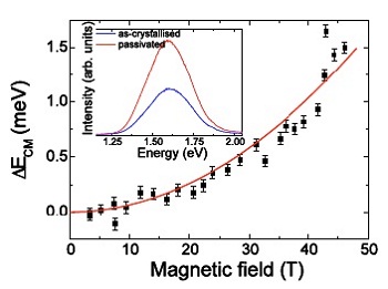
Figure 2: Shift of the photoluminescence (PL) energy for the passivated sample in which there is quantum confinement. The inset shows typical spectrum before (ascrystallized) and after passivation. Note that the PL shift with field is only 1.5 meV and the line width is 300 meV (Courtesy Dr M Hayne, Lancaster University).
The first set of magneto-PL measurements were carried out on an as-crystallised sample; the PL emission was observed to be insensitive to the application of the magnetic field. The sample was then passivated in pure hydrogen at 400ºC, which served to de-activate the defect sites. The emission from the passivated sample was then observed to give the expected shift in the emission wavelength with variation in the magnetic field strength; there was a shift of ~1.5 meV with the application of a 50 T field. This is illustrated in figure 2. It was also observed that the overall intensity of the emission increased. A characteristic parabolic shift was observed (figure 2) with field increase, consistent with a wavefunction extent of ~5 nm. This confirmed that the emission was dominated by QC effects in this case. The researchers then went on to reactivate the defects by exposing the sample to intense UV illumination, which removed the ‘passivating’ hydrogen from the defect sites. The PL data again reverted back to showing no sensitivity to the application of the magnetic field, indicative that the emission was again dominated by it due to the localized defects. The results confirmed that when present, defects are the origin of the bulk of the emission within Si nanocrystals, and when there are no defects the emission is dominated by quantum confinement effects within the nanostructure.
EM technology as implemented on Andor’s iXon platform, successfully met the major challenges posed by such an experiment, namely the sensitivity to measure extremely weak PL signals, and the speed to allow for averaging over a large number of spectral acquisitions.
Graphs courtesy of Dr Manus Hayne, Lancaster University, England.
Date: July 2020
Author: Andor
Category: Case Study
