Resources
 Part of the Oxford Instruments Group
Expand
Collapse
Part of the Oxford Instruments Group
Application Notes
Author: M. Liang, A. A. El Yumin, J. Ye, Zernike Institute for Advanced Materials, University of Groningen
Published: 01 Apr 2018 · Last updated: 10 Jul 2025
Tags: spectro-detect-solutions-ar, luminescence-app
Introduction
In the last decade, two-dimensional (2D) transition metal dichalcogenides (TMDC) have attracted a lot of attention because the same graphene protocol can also be applied to this layered compound to prepare atomically thin flakes easily.
The property of materials can change drastically with the decrease of the thickness of 2D TMDCs. For example, the bandgap of MoS2 changes from indirect to direct when the 2D crystal is thinned down to a monolayer.
This change of bandgap results in a lot of novel properties like the great enhancement of photoluminescence (PL) and valley polarization, a unique spin texture formed in the k-space of the Brillouin zone, which were absent in multilayers. [1]
This rich flexibility between material property and thickness makes TMDC monolayers a class of popular materials in the field of 2D materials. For a typical TMDC, the monolayer is promising for optical experiments because of its narrow direct bandgap and large quantum yield. Here, we studied the Raman Spectroscopy and photoluminescence property of the monolayer.
Experimental set-up
The monolayers were fabricated by the chemical vapour deposition (CVD) method [2]. The Raman and photoluminescence (PL) spectra of were measured using an Andor spectrograph Shamrock SR-500i-D1 and Andor CCD detector iDus DV420A-OE with a field effect gating. The laser excitation was from a Cobalt Samba 532 nm laser.
Results
Figure 1 shows the Raman Spectrum of as-grown flakes. The E2g and A1g peaks were identified at 348 and 415 cm-1, respectively. The insert of Figure 1 plots the PL of flake. A sharp photoluminescence peak is observed at around 632 nm. All these characteristics indicate that the monolayers grown by CVD are high quality. With these monolayers, a field effect transistor with ionic liquid gating was fabricated. [3]
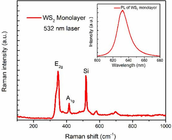
Figure 1: Raman Spectrum of monolayer. Insert, photoluminescence of monolayer.
On high-quality monolayer devices, the electrical driven PL spectra at various liquid gating voltages (-6 to 3V) was tested at 220 K in a vacuum. As shown in figure 2, (a) and (b) correspond to the forward and back sweep of gate voltages, respectively. The gate-dependent shifting of spectra provides information about the exciton and trion formed in the electrically driven PL, which gave us a better understanding of the optical properties of the monolayer.
Conclusion
With the help of the Shamrock 500i spectrograph and the iDus 420 CCD detector, the Raman spectrum and the PL spectra of monolayer as a function of liquid gating voltage can be successfully characterized.
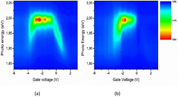
Figure 2: PL spectra under electric field generated by liquid gating: (a) forward sweep, (b) back sweep.
References

© Oxford Instruments 2026
