Resources
 Part of the Oxford Instruments Group
Expand
Collapse
Part of the Oxford Instruments Group
Application Notes
Author: WITec GmbH
Published: 10 Feb 2021 · Last updated: 28 May 2026
Tags: ms-semiconductors-app, rs-app
Silicon (Si) plays an important role in semiconductor devices. During manufacturing, the structures in Si are traditionally generated using lithography. Confocal Raman and Photoluminescence (PL) imaging are useful tools for quality assurance to investigate stress and stress induced artifacts in Si of semiconductor devices. This application note describes the performance of system laser scribing, confocal Raman imaging and confocal PL imaging on a crystalline Si sample with a single microscope system.
Silicon (Si) is the material most widely used for integrated circuits as well as solar cells. Traditionally the structures in these semiconductor devices are produced using lithography. In order to ensure the highest quality, the production steps need to minimize stress and stress induced artifacts. It has been shown [1,2] that Raman measurements can effectively probe the strain state of crystalline materials and thus provide an effective, non-destructive way of developing the most appropriate production processes. Furthermore stress and crystallinity in Si have a strong effect on the Photoluminescence (PL) signal of the Si.
Results and Discussion
All experiments were performed using an Alpha300 RA Confocal Raman Microscope from WITec GmbH.
For the lithography experiments the system was equipped with a 532 nm, 15 mW pulsed laser for laser scribing in combination with the DaVinci Lithography package. The lithography process for writing the structure took approximately 2 minutes.
A planar confocal Raman imaging scan in XY direction (50 x 50 μm2; 200 x 200 points) was performed on the laser scribed area using an additional 532 nm laser (frequency-doubled Nd:YAG) with 20 mW optical power output. A 100x NA 0.9 objective was used to focus the laser spot to a diameter of 355 nm. The signal was collected with an Andor iDus visible-optimized DV401ABV with an integration time of 12.2 ms per spectrum.
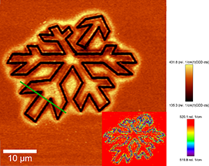
Figure 1: Confocal Raman image of the intensity of the first order Si line. The green line indicates where the depth scan was performed. The insert shows the confocal Raman image of the position of the first order Si line in the planar scan (peak shift).
Following this scan Figure 1 could be extracted from the integrated intensity of the first order Si band near 520 rel.1/cm. The image shows an increased intensity of the Si signal close to the laser scribed structure as well as a strong decrease exactly along it. The insert shows the color coded confocal Raman image of the position of the first order Si line (peak shift). It displays strained sample areas.
The brighter and darker areas in Figure 1 suggest differences in the height of the sample. In such a case the brighter areas could be lying in an optimal focal plane and the dark areas in planes that are not well in focus. In order to check this, a depth scan in the XZ plane (20 x 5 μm2; 200 x 50 points) was performed along the line marked in green in Figure 1. The result can be seen in Figure 2 where the integrated intensity of the first order Si peak is shown. It can be clearly seen, that the intensity originates from approximately the same height and that only very little signal is originating from the positions where the laser-scribed structures are. It can additionally be noted that brighter areas are located right next to the structures. This is in agreement with the results shown in Figure 2.
Figure 2: Confocal Raman Image of the intensity of the first order Si line along a depth scan.
For confocal PL imaging a specially selected 50x NA 0.8 objective was chosen. This allowed the best throughput for the PL signal (in the range of 1000-1250 nm for Si) while showing minimal chromatic aberration between the excitation wavelength (532 nm) and the PL peak.
The detector used for the detection in the Short-Wave Infrared region was an Andor iDus InGaAs DU491A-1.7 camera. A confocal PL scan of the laser scribed structures was performed (50 x 50 μm2, 100 x 100 points, 0.210 s integration time per spectrum).
Figure 3a shows the integrated intensity of the Si PL signal and Figure 3b the PL spectrum itself. This spectrum was acquired right in the centre of the structure. The second order peak of the excitation wavelength at 1064 nm can also be seen in this spectrum. Since Si is an indirect semiconductor, the PL efficiency is extremely low compared to i.e. GaAs. Therefore, only a highly effective detection beam path allows the measurement of the PL signal from a diffraction-limited point with integration times similar to those necessary for Raman imaging.
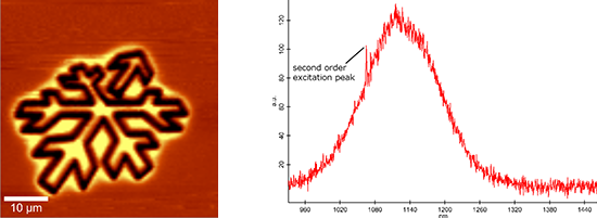
Figure 3: Confocal PL image of the intensity of a PL signal in a planar scan (a) and a representative PL spectrum which originates from the center of the structure (b).
Similar to the previously seen confocal Raman image (Figure 1), the intensity of the signal is stronger close to the structures. It has been shown, however, that more elaborate fitting models also allow the extraction of the stress in Si structures from the PL signal [4].
References

© Oxford Instruments 2026
