Resources
 Part of the Oxford Instruments Group
Expand
Collapse
Part of the Oxford Instruments Group
Application Notes
Author: T. Wecker, M. Deppe, D. Reuter, D. J. As, Department of Physics, University of Paderborn
Published: 01 Feb 2016 · Last updated: 15 Jul 2025
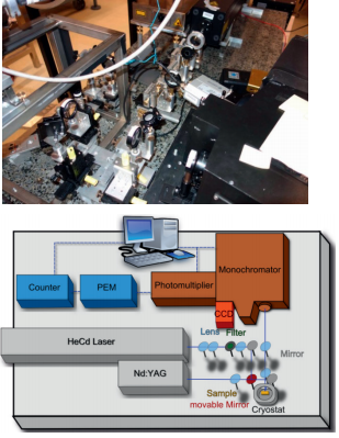
Figure 1: Photoluminescence set-up.
The material system of the group III-nitrides has several advantages, for example the high endurance against mechanical, thermal, and chemical stress. However, common hexagonal group III-nitrides suffer from large internal polarization fields along the c-axis resulting in a bending of the bands and the quantum confined Stark-effect. Due to these effects the design of modern devices for intraband transitions in the hexagonal phase is reasonably complicated caused by the extended number of degrees of freedom involved [1]. Besides, the efficiency of devices based on interband emission is reduced, due to the spatial separation of the electron and the hole wave function. In order to reduce these effects the growth of hexagonal nitrides in semi-polar directions is intensively investigated [2]. Another approach to avoid these restrains is the growth of cubic group III Nitrides in the (001) direction on a suitable substrate like 3C-SiC (001). Hence, all unfavorable effects listed above can significantly be suppressed that way.
Set-up
In this application report we refer to photoluminescence investigations of cubic GaN (cGaN). The temperature dependence of the photoluminescence is used to determine the exciton binding energy of a cubic GaN epilayer. A 600 nm thick cubic GaN epilayer was grown by plasma-assisted molecular beam epitaxy (PAMBE) on a 10 µm thick 3C-SiC (001) layer deposited on a 0.5 mm thick Si substrate. The applied growth system comprises a Riber32 radio-frequency plasma-assisted molecular beam epitaxy. More details on the growth of cubic GaN on 3C-SiC substrates can be obtained in Ref. [3]. An rms surface roughness of cGaN of around 5-7 nm for 5x5 µm2 areas is measured by Atomic force microscopy (AFM) measurements. The structural sample properties were obtained by high resolution X-Ray diffraction (HRXRD) measurements yielding reciprocal space map (RSM). An average dislocation density of the order of D≈1010 cm-2 was estimated from the measured rocking curve full width at half maximum around the (002) reflection. The photoluminescence spectroscopy (PL) setup is shown in Fig. 1.
Two CW lasers can be used for excitation. By moving a mirror either the light of a HeCd laser (325 nm) or a frequency-quadrupled Nd:YAG laser (266 nm) is exciting the sample positioned in a cryostat. With the cryostat temperature dependent measurements of the PL signal in the range of 13 K to 300 K can be achieved. The PL light is focused to the entrance slit of a Spex 370M monochromator. The two exit ports are equipped with an Andor CCD detector (iDus DU420A-BU2) and a Hamamatsu photomultiplier (943- 02 GaAs). A LabVIEW routine is used to control the monochromator, to operate the temperature controller, and to record the measured data from the CCD and the photomultiplier.
Results
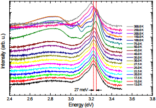
The PL spectra taken with the CCD at different temperatures are plotted in Fig. 2.
For better visualization the spectra are shifted vertically. The c-GaN sample was excited by the Nd:YAG laser with a power of 5 mW and the CCD integration time was 10 ms. First with increasing temperature a clear blue shift of the peak at about 3.22 eV is observable, indicating the thermalization of the bound exciton into the free exciton. The red shift of the free exciton at higher temperature is due to the band gap reduction with temperature and follows the well-known Varshni behavior. With these measurements the exciton binding energy can be determined. Typical values for the exciton binding energy in cubic GaN are 24-28 meV [4]. The additional peaks at lower energies are due to stacking faults and residual C impurities [5].
References

© Oxford Instruments 2026
