Resources
 Part of the Oxford Instruments Group
Expand
Collapse
Part of the Oxford Instruments Group
Application Notes
Author: S. Kühn, Max-Born-Institute for Nonlinear Optics and Short Pulse Spectroscopy im Forschungsverbund Berlin e.V
Published: 01 Apr 2015 · Last updated: 28 May 2026
Tags: material-science-app, ms-semiconductors-app, nl-spectroscopy-app
The development of optoelectronic devices for use in the UV/blue region is enhanced by a better understanding of the properties of the available wider bandgap semiconductor materials. Of particular interest is the study of excitons and their characteristics when generated in thin films of suitable materials. Zinc oxide (ZnO) is one such wide bandgap material undergoing investigation. This short note outlines work by a group at the Max-Born Institute for Non-linear Optics and Short Pulse Spectroscopy [1,2,3] who are investigating the excitonic characteristics of thin films of ZnO using time integrated and time resolved photoluminescence. In one set of experiments they use a 500 mm focal length spectrograph along with a high sensitivity CCD camera (Newton DU920P-OE) to acquire time integrated PL spectra associated with the different types of excitons.
Excitons can be created in semiconductors when a photon is absorbed so as to excite an electron from the valence band into the conduction band, leaving behind an electron hole which in turn behaves like a positively charged particle. Consequently the electron and hole attract each other whilst in this excited state and form what is referred to as a quasi-particle, which is essentially neutral electrically, and that can move about within the semiconductor material. As a result excitons can cause the transport of energy within the crystal before the energy is lost by a number of means such as radiative recombination, or exchange processes within the lattice.
Zinc oxide receives increasing attention as a semiconductor material for UV/blue electro-optic nano-devices. Among the reasons are the high exciton binding energy of 60 meV, the bandgap of 3.3 eV, the radiation resistance, low production cost and non-toxicity. Recent advances in ZnO fabrication by radical-source beam epitaxy make high quality films available, that permit the study of excitations in the surface region of the crystal. While the bulk of a semiconductor can be modified and structured by doping and alloying, the semiconductor surface offers the possibility of modification through a much wider range of materials, in particular organic molecules. The interaction may be static or dynamic, including energy and charge transfer or even strong coupling and hybridization. The latter types of interaction sensitively depend on the separation between the excitons in both materials and on their dimensionality (1D or 2D).
There exists a specific excitonic state on high quality ZnO films, that is localized just a few nm below the surface, known as the surface exciton (SX). It is often the dominant excitonic feature in ZnO nano-structures at low temperatures. At first glance the SX looks like the perfect candidate for hybridization with organic crystals. But is it really?
To find out, the researchers looked into the spatially resolved spectral and dynamic properties of the SX at the nanometre length scale. They utilized a near-field scanning optical microscope (NSOM) operated at variable temperatures down to 5 K. Using photoluminescence (PL) imaging, a spectral map of the SX excitons was acquired and compared with similar maps for another ubiquitous excitonic state, the neutral donor-bound exciton (DX). A spectral map is shown later in figure 3.
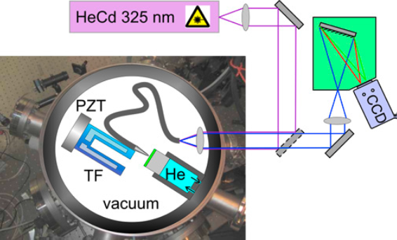
Figure 1: Schematic diagram of the setup with the optical path and the vacuum chamber housing the NSOM. The near-field tip is glued to a quartz tuning fork and mounted on a 3D piezo translation stage. He: liquid helium flow cryostat, TF: tuning fork, PZT: piezo scanner.
Perhaps the most common NSOM is based on light confinement by a nanoscopic aperture in the metallic coating of a pointed optical fibre tip. However, to avoid problems with poor transmission and quenching by the metal, they used all-dielectric tips that achieve a good resolution of ~λ/3 (at 370 nm) combined with near unity transmission. This allowed the system to be used in excitation - collection mode, where the PL is collected through the same tip that is used for excitation, thus simplifying the optical setup. Using a shear-force feedback, the tip was positioned ~10 nm above the sample surface, which thereby prevented immediate contact of the tip with the delicate surface. An electron micrograph of the tip is shown in Figure 2.
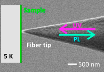
Figure 2: Electron micrograph of a dielectric NSOM tip with the schematic of the measurement geometry.
The excitation light was delivered from a HeCd laser (wavelength 325 nm, 3.81 eV). Spectra were acquired with a 50 cm focal length spectrograph (ACTON, SpectraPro 2500i), incorporating a grating with 3600 lines/mm, and a thermoelectrically cooled CCD camera (Andor Newton). The main requirements of extremely low mechanical vibration, high sensitivity in the near UV, low background current and good uniformity were essential to this experiment. It must be remembered that the small detection volume delivers a proportionally small signal that cannot be compensated by an increased excitation energy/power without driving the excitonic PL into a non-linear regime.
To observe the spatial properties of excitons near the ZnO surface, a special sample was grown consisting of a 20 nm ZnO thin film and a 350 nm Zn0.88Mg0.12O blocking layer on a ZnO substrate. The blocking layer absorbs all photons that are transmitted through the thin film and prevents them from reaching the substrate. Thus, all photons in the signal ZnO PL band could be considered to originate from the thin film only. Consequently, the thin film represented a nanostructure with a high ‘surface area-to-volume’ ratio, but in a clear two-dimensional geometry. The thin film was furthermore decorated with a monolayer of stearic acid. This molecule is known to enhance the SX excitations on the ZnO surface through its COOH anchor group. The chemisorbed molecule acts as a surface impurity capable of binding an exciton to the surface with localization energy around 10 meV; this corresponds to resonance energy of 3.3665 eV.
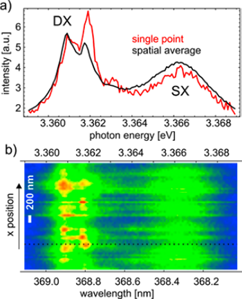
Figure 3: a) Spatially averaged (black) and single point (red) spectra of the ZnO thin film showing the DX and SX resonances. b) Spatially resolved spectra over 2.8 μm showing the DX fine structure. The dotted line corresponds to the spectrum shown in (a). Fluctuations of the intensity at some scan positions are caused by mechanical vibrations of the flow cryostat.
In Figure 3a the spectral signature of the SX can clearly be recognized. The width is around 6 meV. In addition, there is the ubiquitous DX resonance at 3.3615 eV corresponding to an exciton bound to a neutral donor common to most ZnO crystals. Sharp lines limited by the instrument resolution of 0.5 meV can be observed here. As shown in the spatially resolved spectrum in figure 3b, the DX lines are spatially localized and fluctuate in energy. At the same time, the SX remains broad and featureless, just as in the case for the spatially averaged spectrum. Hence, it can be concluded that the character of the SX differs from the common DX in terms of the localization behaviour.
It may be argued that the resolution of 100 nm (∼λ/3, Sparrow criterion [4]) is insufficient to resolve individual SX resonances. However, the temperature dependence of the SX lifetime τ(T) and a time-resolved transport measurement IPL(t) provide evidence that the SX is delocalized and two-dimensionally extended. The transport was observed from the shortening of the SX lifetime under the local excitation and local detection scheme provided by the NSOM. Diffusion of excitons out of the detection area acts like an additional decay channel for the exciton population that is initially created during the excitation.
The two-dimensional character of the SX is beneficial for the coupling to organic crystals deposited on top of the ZnO since the distance dependence of the coupling strength is more relaxed than in the case of two point-like dipoles. Consequently the SX exciton is a hot candidate for future hybrid optoelectronic nano-devices.
High quantum efficiency paired with a low background noise, easy integration into the NSOM system with a control program based on LabView, and a high degree of flexibility are distinguishing qualities of the Newton camera that was used for these challenging measurements.
The information and figures for this note have been gratefully received from Dr Sebastian Friede, Max-Born-Institute for Nonlinear Optics and Short Pulse Spectroscopy im Forschungsverbund Berlin e.V., Berlin.

© Oxford Instruments 2026
