Resources
 Part of the Oxford Instruments Group
Expand
Collapse
Part of the Oxford Instruments Group
Application Notes
Author: C. Weber, J. Pahl, S. Bommel, S. Kowarik, Institute of Physics, Humboldt University, Berlin
Published: 01 Feb 2012 · Last updated: 16 Jul 2025
Tags: ms-semiconductors-app, absorption-app
Organic semiconductor thin film devices are promising candidates for a large variety of optoelectronic applications such as OLED displays and semi-transparent solar cells. Among other advantages, organic semiconductors offer the possibility of changing the optical properties of a thin film drastically by chemically altering the molecular structure, or by physically changing the molecular arrangement through choice of suitable growth conditions [1]. In this work we study the optical properties of ultrathin films of the organic semiconductor diindenoperylene (DIP, C36H16, Figure 1). DIP provides charge carrier mobilities up to 0.1 cm2/Vs, long exciton diffusion length and power conversion efficiencies of about 4% in organic solar cells [2].
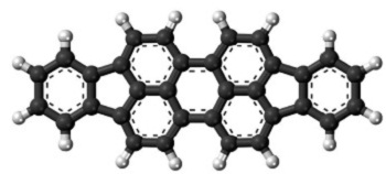
Figure 1: Structure of diindenoperylene (DIP)
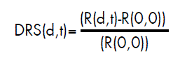
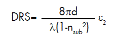
Since the growth mode of the first monolayer will influence the crystal structure of the whole film, a highly sensitive measurement setup is necessary to monitor the growth process from the first sub-monolayers onwards. One optical method that has proven to be sensitive enough to detect single monolayers is differential reflectance spectroscopy (DRS) [3,4,5]. In DRS the reflectivity of the thin film R(d,t) as well as the reflectivity of the bare substrate R(0,0) is measured and normalized according to the following formula:
Our DRS measurement setup consists of a 75 W Xe-lamp with passive cooling for high power stability (LOT-Oriel) and a PI Acton spectrometer in combination with an Andor Technology Newton DU920P-OE CCD detector. The sample is prepared by thermally evaporating DIP-molecules onto a glass substrate in high vacuum (HV). The optics setup is coupled to the vacuum chamber via an optical fibre with a reflection probe (LOT Oriel) (Figure 2).
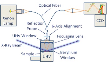
Figure 2: Experimental setup for DRS measurements. The optics is coupled to the UHV chamber via an optical reflectance fiber. The light is focused onto and collected from the sample with a lens.
The ultra-portable vacuum chamber is equipped with a quartz glass window on top and a beryllium window around the sample holder to allow simultaneous x-ray scattering and optical spectroscopy experiments during organic molecular beam deposition OMDB (organic molecular beam deposition). In combination with a laser diode, the optics setup can also be used for in situ fluorescence and Raman spectroscopy due to the high sensitivity of the CCD.
The glass substrate was roughened on one side to avoid back side reflections and cleaned with Isopropanol and ultrapure water in an ultrasonic bath. The film was grown with a rate of approximately 3 nm/min.
Our DRS setup allows us to take the DRS signal in-situ and in real-time during OMBD growth. To achieve high sensitivity and good time resolution in differential reflectance spectroscopy a large dynamic range of the CCD is necessary, because detection of small differences in the large reflectivity signal requires detection of high photon numbers. In most cases the time resolution is below one second. The acquisition time is approximately 1 ms but averaging over 1000 spectra is used here to improve the signal-to-noise ratio.
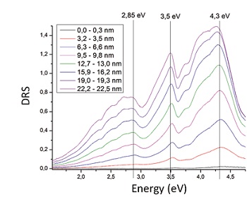
Figure 3: DRS spectra of DIP taken during growth. 1 monolayer corresponds to a thickness of about 1.7 nm.
In Figure 3 the temporal evolution of the DRS signal during growth of DIP on glass is shown. All features exhibit a slight redshift as the film gets thicker. Of interest is the mode at 2.85 eV, which in the literature is referred to as the fourth mode of DIP and grows stronger with increasing film thickness. It has been proposed that Frenkel excitons might cause this thickness dependent behaviour of the fourth mode [6]. One can also identify the vibronic progression of the lowest energy π - π *-transition, appearing as three broad peaks at 2.25 eV, 2.45 eV and 2.65 eV.
Furthermore there are two strong absorption features in the UV-region at 3.5 eV and 4.3 eV, that have not been observed yet.
A good signal-to-noise ratio of the measured DRS signal can be obtained even for film thicknesses = 1.7 nm, that is below 1 monolayer of DIP. The absorption spectrum can be extracted from the DRS signal by fitting the DRS data with a fitting routine based on the matrix formalism for wave optics [7]. This formalism can be simplified in the limiting case of film thicknesses far below the wavelength λ and transparent substrates, and ε2 can be directly calculated from the DRS signal by evaluating the equation
With nsub being the refraction index of the substrate, d the film thickness and λ the wavelength. Using this approximation for a sub-monolayer DIP film, the imaginary part of the dielectric constant ε2 shown in Figure 4 can be extracted from the DRS measurement. Four weak modes are present between 2.25 eV and 2.85 eV, while stronger absorption features are observed at 3.5 eV and 4.3 eV. Even thicknesses below 3 Å provide a signal-to-noise ratio >12, This means that dielectric properties can be studied for ultrathin films.
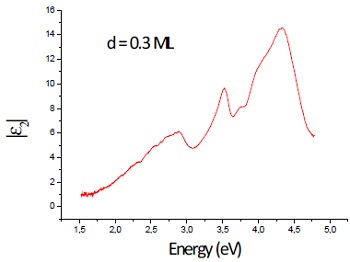
Figure 4 : Imaginary part of the dielectric constant of DIP on glass in the region below 1 monolayer. The absorption properties are important for applications such as organic photovoltaics
With our new optical setup we were able to obtain time-resolved in situ DRS spectra during DIP film growth on glass for thicknesses between 0.1 and 14 monolayers with excellent sensitivity and a time resolution of one second. We found very strong absorption features in the UV region, present even for ultrathin film thicknesses below 1 monolayer.
This setup serves as a standard in-situ monitoring tool of molecular thin film growth with good time resolution. In addition, the highly sensitive detection opens up even more possibilities such as optical measurements of self-assembled monolayers or real-time Fluorescence and Raman spectroscopy during film growth when using laser illumination.
The information and figures for this note have been gratefully received from Prof Stefan Kowarik, Humboldt University of Berlin, Institute of Physics.

© Oxford Instruments 2026
