Resources
 Part of the Oxford Instruments Group
Expand
Collapse
Part of the Oxford Instruments Group
Case Studies
Author: S. Brüninghoff, Merck KGaA, Dept SO-ACP-7, Darmstadt
Published: 01 Apr 2015 · Last updated: 28 May 2026
Tags: luminescence-app, ms-semiconductors-app
Organic light-emitting diodes (OLEDs) are devices which emit light when electric current is passed through them. They are similar to standard LEDs except that the electroluminescent layers consist of thin films of organic compound. OLEDs are used to create digital displays in devices such as computer monitors, screens in mobile phones, and television. This note outlines work being carried out by a group at the Department of OLED Research at Merck KGaA [1], using a spectrograph and ICCD camera to measure photoluminescence, with a view to understanding the fundamental behaviour of such materials at a range of cryo-temperatures.
OLEDs can be manufactured as monochrome (red, green, blue) opto-electronic devices as well as white-emitting by mixing materials [2]. Additionally, these materials can be applied as amorphous layers onto any substrate, which, due to non-existent lattice strains, leads to a mechanical flexibility. Apart from these desirable mechanical properties the superior optical properties are also of interest for the display industry. However, OLED materials tend to age and lose their efficiency at different rates. Consequently, it is important to understand the fundamental internal processes of these materials in order to improve them.
Unlike inorganic semiconductor systems, in which the properties are influenced by variation of dopants for example, the properties of organic materials are modified directly by modifying the structure of the molecule.
Layers with different functions are needed in the production process of organic LEDs. Depending on the function, these layers must have different optical properties. Optimization of the physical properties of the individual layers can improve the efficiency of the overall OLED system. Such optimization will be based on knowing and understanding the properties of the individual layers.
In order to garner this insight the group investigated the first excited singlet (S1) and triplet (T1) states and the positioning of their levels. The decay times of the fluorescence and phosphorescence associated with these states were used to assess the important properties of the OLED material.
A measurement system for the determination of triplet energy and decay times of light-emitting layers was set up with the goal of optimizing the efficiency of the materials for the different layers. The aim of the experiment was to measure the integrated intensity of the T1 level at low temperatures and the temporal evolution of this level.
The data obtained provided information on the path and the diffusion velocity of excitons as well as the interactions between the different energy levels. Moreover, it was possible to investigate the thermal behaviour of the materials making up the OLED system.
The measurement setup consisted of the following main components:
The laser (CryLas FQSS 266-200) was a three-fold double pulsed ND:YAG laser operating at a wavelength of 266 nm. The pulse energy of the laser was 200 µJ with pulse width of 1.5 ns. A beam expander was installed between the laser and the sample chamber. A schematic of the setup is shown in Figure 1.
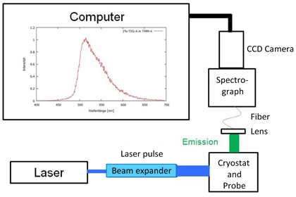
Figure 1: Schematic layout of the measurement station.
The sample chamber (Oxford Instrument Optistat DN-V2) incorporated liquid nitrogen cooling and was evacuated for thermal isolation. It was mounted at the end of the cryostat column and had four windows through which the sample could be irradiated with the excitation light and the emission light could be coupled into an optical fiber using a collimating lens. The glass fiber delivered the light signal to a spectrograph (Andor SR-303i-A), where it was dispersed on to the multichannel detector (Andor ICCD iStar 320). A picture of the experimental setup is shown in Figure 2, with the spectroscopy system in the background and the cryostat and chamber on the right.
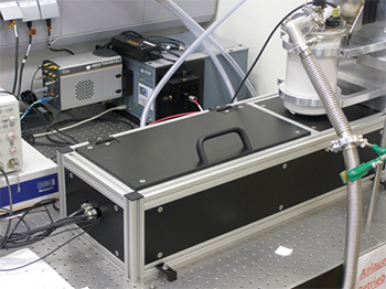
Figure 2: A picture of the measurement setup showing the spectrograph and ICCD camera in the background.
When taking a measurement, the laser was initially fired such that it delivered a pre-trigger pulse to the camera for synchronisation. The propagation delay in the setup was ~ 72 ns so the system was configured to capture the second and every successive pulse but ignoring the initial laser pulse. The software controlling the camera facilitated accurate and easy control of the delays for synchronisation.
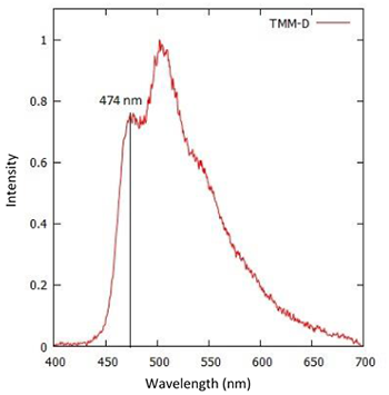
Figure 3: Emission spectrum of an OLED material
Labview Software Developer Kit along with an in-house custom application enabled an integrated system with full control of all components. The ‘kinetic series’ mode of acquisition along with the use of the camera ‘gate step’ utility enabled a series of spectra to be acquired with varying delays between the laser excitation and acquisition of the optical emission. This enabled the decay times to be deduced from the evolution of the light emission. Multiple acquisitions were performed and averaged to get a good signal-to-noise ratio measurement.
An emission spectrum of an OLED material is shown in figure 3. The evaluation of the T1 level was carried out by assessing the intensity at the first maximum peak located at 474 nm in Figure 3.
Figure 4 shows a time series for the intensity at 474 nm as it decays over time. This represents the time dependent course of the emission originating from the recombination of excitons with T1 levels. Since fluorescence and phosphorescence are overlapping and the early emission is associated with fluorescence and the later emission with phosphorescence, we can assess the time dependent course of the phosphorescence by focusing on the emission in the later part of the characteristic; this is highlighted as the section marked by the blue bar in Figure 5.
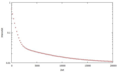
Figure 4: Measurement of a sample's decay time. This is based on the decay of the intensity at 474 nm.
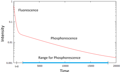
Figure 5: Decay curve for the phosphorescence.
The properties of the triplet-triplet-annihilation (TTA) of the OLED materials can be determined by fitting a mathematical model to the time dependent course of the phosphorescence. This is illustrated in Figure 6. As the fluorescence has a disruptive or interfering effect on the measurement of low phosphorescent OLED materials, the camera utilises a "boxcar" mode, which introduces a delay time before the start of the acquisition, so that the quickly disappearing fluorescence is ‘rejected’ and not acquired by the camera. After that, the sensor of the camera is exposed until the next laser impulse is present. Using this technique, spectra of very low phosphorescence could also be recorded.
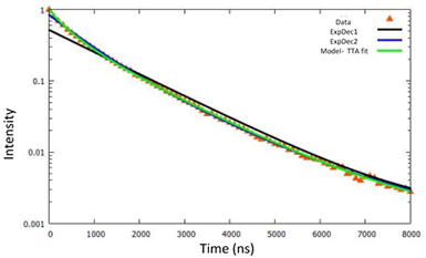
Figure 6: Determination of the triplet-triplet-annihilation. The modelled fit to the decay curve is shown in green.
Figure 7 shows three spectra of another OLED material that have been recorded with different delays. The first spectrum (red) was recorded at the time of t = 0. It shows the typical fluorescence spectrum of the OLED material. When a delay is introduced a second peak can be identified. This second peak corresponds to the phosphorescence. This shows how a very strong fluorescence signal can dominate the total emission which could prove challenging for the measuring low phosphorescence OLED materials especially where there is significant overlap between the two types of emission; consequently this poses problems for the measurement of the T1 levels. However, with the faster decay time of the fluorescence and the capabilities of the camera in terms of controlling timing delays (and acquisition gating), it was still possible to measure very low phosphorescence signal, as demonstrated by the blue curve.
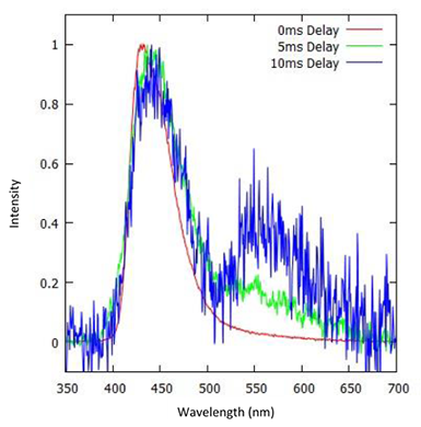
Figure 7: Normalised spectra of a low phosphorescent OLED material with different delay times.
In summary the group have demonstrated how an ICCD camera (Andor iStar) can be used to achieve very good measurements of OLED emission spectra (even for low phosphorescent samples), including decay times for emissions in the wavelength range of 350 - 700 nm and acquisition times (and delays) with time intervals ranging from nanoseconds up to seconds. This enabled them to characterise material layers used in OLEDs for their low-temperature properties such as the triplet-triplet-annihilation and the temperature dependence of the decay profiles.
This information and figures for this note have been gratefully received from Dr Sven Bruninghoff, Merck KGaA, Dept. SO-ACP-07, Darmstadt, Germany.

© Oxford Instruments 2026
