Resources
 Part of the Oxford Instruments Group
Expand
Collapse
Part of the Oxford Instruments Group
Application Notes
Author: Dr. Claudia Ruppert, Experimentelle Physik 2, Technische Universität Dortmund
Published: 01 Jul 2015 · Last updated: 10 Jul 2025
Tags: ms-semiconductors-app
Since the discovery of graphene, atomically thin quasi two-dimensional materials have been studied very intensely in the past decade.1 They often exhibit very unique fundamental properties which strongly differ from the corresponding bulk or multi-layer form and research has extended towards their use in functional devices. The best studied materials so far are members of the family of transition metal dichalcogenides (TMDs). These materials with the chemical formula MX2 consist of a transition metal M of group IV, V or VI (e.g. Ti, V, Mo) and chalcogenide atoms X (S, Se, Te). Many of these TMDs have a layered structure where strongly bound atomic sheets are held together by weak Van der Waals’ forces to form a crystal which strongly facilitates the cleavage down to single layers by mechanical exfoliation.
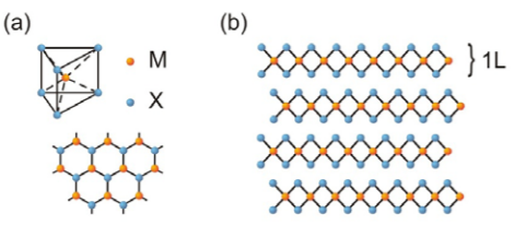
Figure 1: Crystal structure of MX2 based transition metal dichalcogenides.
The crystal structure of MX2 is composed of hexagonal sheets of M atoms that are sandwiched between two hexagonal planes of X atoms, with trigonal prismatic coordination [Figure 1 (a)]. These X-M-X units, which are generally referred to as monolayers (1L), are held together by Van der Waals’ forces and are stacked with 2H symmetry [Figure 1 (b)]. In general the thickness of a monolayer is about 0.7 nm and sheet dimensions lie in the range of a few µm2 for mechanically exfoliated specimens. Within the group of these TMDs bulk MoTe2 is a semiconductor with an indirect band gap of about 1.0 eV. For the monolayer a direct optical band-gap at 1.095 eV has been found.(2) Since this spectral regime is close to or beyond the capability of silicon detectors, the use of InGaAs based technology for the characterization of atomically thin films of MoTe2 is much more suitable.
The samples consist of mono- or few layers of MoTeTe2 exfoliated mechanically onto a quartz substrate. To characterize the photoluminescence (PL) of these samples they are embedded into a µ-PL setup schematically shown in Figure 2. For excitation a solid state cw-laser with a wavelength of 532 nm is focused onto the sample with a 100 x 0.95NA microscope objective resulting in a diffraction limited spot size. The collection of the PL from the sample is achieved in reflection geometry by the same objective. Here a high NA objective is essential to collect as much emission as possible. Due to the small material volume and the limited excitation power given by the damage threshold of the sample, the intensity of the PL emission of a monolayer is very low. The PL is detected by a spectrograph (Kymera-193i-B1-SIL) equipped with a silver grating with 150 l/mm (1200 nm blaze wavelength) and a photodiode array (iDus InGaAs DU490A-1.7). In front of the spectrometer a filter is used to block the radiation from the excitation laser.
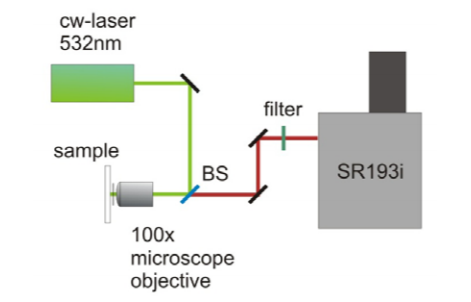
Figure 2: Experimental setup
Figure 3 shows the PL of a monolayer MoTeTe2 sample. The monolayer was excited with a power of 8 µW. The data has been taken with 50 s integration time and an accumulation of 4 spectra. The camera has been cooled down to -60 °C. The maximum of the PL emission lies at 1.09 eV which is very close to the expected optical band-gap. Obviously the PL intensity of the sample is very weak. Due to the high quantum efficiency of the InGaAs photodiode array and its low noise when cooled down the PL can still be measured within a reasonable amount of acquisition time.
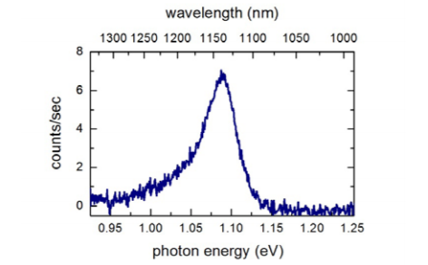
Figure 3: Photoluminescence of monolayer MoTeTe2.
[1] Butler, S. Z.; Hollen, S. M.; Cao, L.; Cui, Y.; Gupta, J. A.; Gutiérrez, H. R.; Heinz, T. F.; Hong, S. S.; Huang, J.; Ismach, A. F.; Johnston-Halperin, E.; Kuno, M.; Plashnitsa, V. V.; Robinson, R. D.; Ruoff, R. S.; Salahuddin, S.; Shan, J.; Shi, L.; Spencer, M. G.; Terrones, M.; Windl, W.; Goldberger, J. E. ACS Nano 2013, 7 (4), 2898– 2926.
[2] Ruppert, C.; Aslan, O. B.; Heinz, T. F. Nano Lett. 2014, 14 (11), 6231–6236.

© Oxford Instruments 2026
