Resources
 Part of the Oxford Instruments Group
Expand
Collapse
Part of the Oxford Instruments Group
Application Notes
Author: Prof. Dr. Monika Fleischer, Institute for Applied Physics and Center LISA+, Eberhard Karls University Tübingen
Published: 01 Aug 2017 · Last updated: 16 Jul 2025
Tags: microspectroscopy-app
Plasmonic nanostructures are widely used in many different research and application areas such as biosensor technology, nano-spectroscopy [1,2,3], nano-photonics and others. This mainly is because they exhibit a strong near-field enhancement that is closely confined to the vicinity of the structures. The optical characterization of plasmonic nanostructures is challenging though, both due to the low light intensities of individual structures, and because multiple broad plasmonic resonances can be excited due to different excitation conditions or multipolar orders, which are not easily separated. As the structures are usually much smaller than the diffraction limit of visible light and their scattering intensity is comparatively low, they cannot be imaged well with a bright-field microscope. Taking transmission spectra also yields low signal-to-noise ratios. To circumvent these problems, dark-field scattering spectroscopy can be used. Here the nanostructures are illuminated in such a way that only scattered light is collected, thus yielding high contrast images and spectra.
The setup for measuring dark-field scattering spectra of single plasmonic nanostructures is shown in Fig. 1. First, a white-light source is focussed onto the surface of the sample.
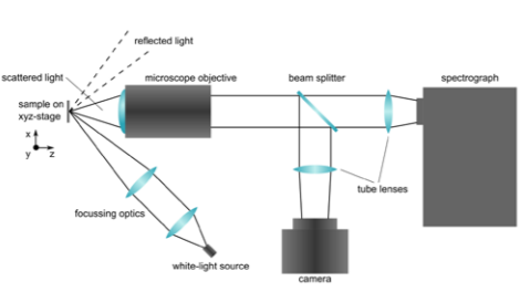
Figure 1: Schematic of the setup used for the automated recording of dark-field spectra of single nanostructures.
Here the illumination angle should be chosen in a way that no reflected light will enter the microscope objective. Only scattered light is then collected by the objective and split up into two paths. One path continues into a camera for imaging, and the other is directed to an imaging spectrograph (Andor Shamrock SR-303i) with a CCD-detector (Andor iDus DU416A-LDC-DD). To check whether a single structure is positioned at the centre of the detector, the spectrograph is used in image mode. Then the motorized slit is adjusted such that only one structure is visible. Using the “Single Track” feature, only the rows of the CCD which correspond to the structure are read out. This way it is possible to obtain the spectrum of a single nanostructure, given that any other structures are sufficiently far away (~ 3 μm for a 50x objective). As the scattered intensity is very low, the high quantum efficiency and the low dark current of the iDus detector are prerequisites for a good signal-to-noise ratio. The sample is mounted on a piezo-stage, and using custom-made software in conjunction with the Andor SDK, it is possible to automatically take spectra of nanostructures that are placed on a regular grid.
Plasmonic nanostructures were fabricated on a regular 5x5 grid by using electron-beam lithography. Two nano-circles in close proximity were exposed at each grid position. Thermal evaporation of gold and subsequent lift-off resulted in high aspect-ratio pillars. Rapid thermal annealing of these pillars leads to the formation of quasi-spherical dimer nanostructures with small gap sizes. In Fig. 2 scanning electron microscope (SEM) images of part of such an array of nanostructures are depicted. At each grid point a single nanostructure with either one (due to limited adhesion in the fabrication process) or two spheres resides.
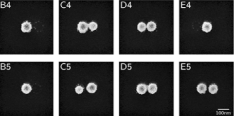
Figure 2: SEM images of different nanostructures that were fabricated as part of a 5x5 array.
Individual dark-field scattering spectra were taken for each structure using the setup described in Fig. 1. The incident light was polarized along the long dimer axis, so only the dipolar mode of the dimers was excited. In Fig. 3 exemplary results for the structures depicted in Fig. 2 are shown. By looking at the signal-to-noise ratio and associating it with the corresponding SEM image, one can see that the dimers have a much higher scattering cross-section than the single spheres. In addition, a closer inspection of the spectra of the dimers reveals that the dipolar mode shows an increasing red-shift for decreasing gap sizes.
![Figure 3: Dark-field scattering spectra (intensity [a.u.] vs. wavelength [400-950 nm]) of the single plasmonic nanostructures shown in Fig. 2. The measurements were taken with the setup shown in Fig. 1. The grey lines represent the raw data, the coloured lines are smoothed to reduce the noise.](https://www.oxinst.com/learning/uploads/inline-images/imagetools1-20210114103006.png)
Figure 3: Dark-field scattering spectra (intensity [a.u.] vs. wavelength [400-950 nm]) of the single plasmonic nanostructures shown in Fig. 2. The measurements were taken with the setup shown in Fig. 1. The grey lines represent the raw data, the coloured lines are smoothed to reduce the noise.
Dark-field spectroscopy is a widely used technique for the optical characterization of nanostructures, and with the addition of an automated setup using the Andor SDK it provides a convenient and reliable method to characterize single nanostructures. Also this enables the characterization of a large number of structures and thereby a statistical analysis of their properties.
[1] C. Schäfer, D.A. Gollmer, A. Horrer, J. Fulmes, A. Weber-Bargioni, S. Cabrini, P.J. Schuck, D.P. Kern, M. Fleischer, Single particle plasmon resonance study of 3D conical nanoantennas, Nanoscale 5,7861 (2013)
[2] A.J. Meixner, R. Jäger, S. Jäger, A. Bräuer, K. Scherzinger, J. Fulmes, S. zur Oven Krockhaus, D.A. Gollmer, D.P. Kern, M. Fleischer, Coupling single quantum dots to plasmonic nanocones: optical properties, Faraday Discussions 184, 321 (2015)
[3] J. Wang, J. Butet, A.-L. Baudrion, A. Horrer, G. Leveque, O.J.F. Martin, A.J. Meixner, M. Fleischer, P.-M. Adam, A. Horneber, D. Zhang, A direct comparison between second harmonic generation and two-photon photoluminescence from single connected gold nan

© Oxford Instruments 2026
