Resources
 Part of the Oxford Instruments Group
Expand
Collapse
Part of the Oxford Instruments Group
Application Notes
Author: Dr. Levent Gütay, Workgroup UND (Ultrafast Nanoscale Dynamics), Institute of Physics, University of Oldenburg
Published: 01 Oct 2020 · Last updated: 16 Jul 2025
Tags: optical-tools-renewable, ms-energy-app, material-science-app
Research on novel thin film solar cells has always been motivated by the low material and energy consumption which is needed for the processing of this type of device. This approach appears promising for establishing more sustainable technologies and reaching shorter energy payback times than for the well-established crystalline Silicon technology. Most thin film approaches are based on heterostructure designs, which include materials of which the lattice constants, band gaps, electron affinities etc. are substantially different. This leads to drastic band discontinuities and barriers which may hamper the formation of a good p-n-structure. For an improved heterostructure an additional thin semiconducting layer is introduced in some technologies, which is often referred to as buffer layer. For CIGSSe and CZTSSe technologies, which contain constituents with comparably low toxicity potential, the rather toxic CdS compound has been traditionally used as the most forgiving and versatile buffer material. During the last few years significant research effort has been carried out in order to search for alternative non-toxic buffer materials and for improving the quality of the heterostructure. Among these InS and Zn(O,S) are the most prominent ones.
In this application note we analyze CZTSSe samples with different buffer layers which were supplied in the context of a recent research project. Besides the mentioned standard CdS buffer, an alternative Zn-based buffer and a hybrid approach were tested, which combines a thin layer of CdS with the Zn-based buffer. We apply the method of calibrated photoluminescence (PL) for extracting the splitting of the quasi Fermi levels, which determines the reachable open circuit voltage (Voc) in a device. This characterization technique also has the advantage that it can predict the effect of the investigated modification already at an early stage in the production process without having to fabricate the complete solar cell.
The PL spectra were measured in a Labram Aramis from Horiba, which is a confocal Raman microscopy setup. The system was modified for PL measurements by adding a dichroic beam splitter to the beam line, which allows us to maintain the original functionality of the system. The collected PL signal was focused into a fiber and guided to the detection unit which contains a Kymera193i-B1-SIL spectrograph with a standard SMA fiber mounting port and a 512 pixel InGaAs camera iDus InGaAs DU490A-1.7 both from Andor Technology.
The detection unit was controlled separately from the Labram Aramis on a second computer system. However, synchronization of both systems for e.g. simultaneous Raman and PL mapping on the same position is possible via external TTL connection between the two units.
The photoluminescence spectra were measured on CZTSSe absorbers with buffer layers. The excitation was performed by a 532 nm semiconductor laser at a laser power of < 3 mW, whereas the laser power during measurement was reduced to exclude possible bleaching/degradation effects on the sample, while keeping it sufficiently high for obtaining a good signal-to-noise ratio. For obtaining spectrally calibrated measurements, the spectrum of a white light calibration lamp was measured prior to PL for obtaining a spectral correction function for the recorded PL data. It should be noted, that such calibration spectra have to be obtained for all configurations/settings of the systems, i.e. different center wavelengths of the spectrometer/ detector, optical filters, objectives etc. For this purpose the calibration lamp is placed next to the sample stage and a white reflection standard is placed instead of the sample.
A set of measured PL spectra is plotted in Fig. 1. The plots show mainly the high energy parts of the spectra, which are used for the evaluation. According to Planck’s generalized law [P. Würfel, J. Phys. C 15 3967 (1982)] the light emission from a semiconductor is a function of the splitting of quasi-Fermi levels, sample temperature, and absorbance, which can be expressed in a simplified way as
with A: absorptivity, Ephot: photon energy, QFLS: splitting of quasi-Fermi levels. For A=1 and Ephot » kT the expression can be further simplified and written as
In this case this expression is valid for photon energies >1.05 eV, where A saturates around unity, due to the high absorption coefficient and used thickness of the measured CZTSSe absorbers. In fig 2 the same spectra are plotted in log scale after division by E2phot.
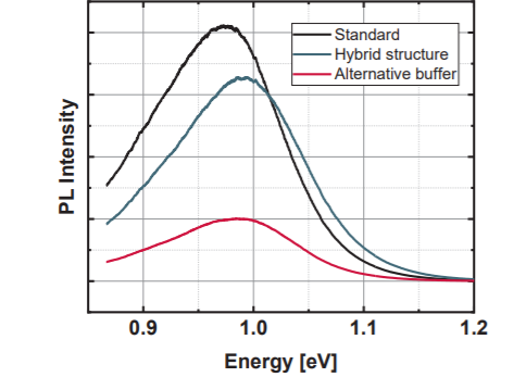
Fig.1
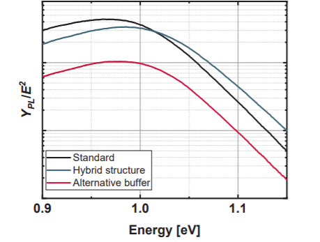
Fig.2
The high energy part of the spectra then accordingly follows the linear behavior in eqn. 2. The evaluation of the spectra shows a clear reduction of the splitting of the quasi-Fermi levels of more than 30 meV for the alternative buffer when compared to the standard CdS buffer. This result indicates either a worse passivation of the absorber/buffer interface or the introduction of new defects by the alternative buffer. The application of the hybrid structure on the other hand shows a clear enhancement of the splitting of quasi-Fermi levels by around 20 meV when compared to the standard configuration. This could be explained by an improved passivation of interface states. The larger splitting of quasi-Fermi levels can be considered as an enhancement of the overall quality of the photo-excited state and as mentioned can be expected to result in a higher Voc in the final solar cells.
Finally, solar cells were fabricated based on similar absorbers, confirming the qualitative trend in Voc, which was predicted by the extracted trend of the splitting of the quasi-Fermi levels from the PL measurements. In detail, the discrepancy, which was observed between the quantitative numbers from PL and electronic measurements on the device, implies that the interface formed with the alternative buffer obviously suffers more dramatically than predicted by PL, indicating the formation of additional transport barriers, which show their impact only in the electronic measurements on final devices. The predicted improvement of Voc for the hybrid approach was confirmed by measurements on the device, indicating that the main improvement of the cells resulted from an improved passivation of the interface states, resulting in a larger splitting of quasiFermi levels.
David Regesch, Levent Gütay, […], and Susanne Siebentritt, Appl. Phys. Lett. 101, 112108 (2012), Degradation and passivation of CuInSe2.
Levent Gütay, David Regesch, […], and Susanne Siebentritt, Appl. Phys. Lett. 99, 151912 (2011), Influence of copper excess on the absorber quality of CuInSe2.
Thomas Unold, Levent Gütay, Wiley, Book chapter 11: Photoluminescence Analysis of Thin‐Film Solar Cells, Book: Advanced Characterization Techniques for Thin Film Solar Cells

© Oxford Instruments 2026
