Resources
 Part of the Oxford Instruments Group
Expand
Collapse
Part of the Oxford Instruments Group
Application Notes
Author: Prof. Dr. Karl, Unterrainer Technische Universität Wien Photonics Institute, and University of Münster Institute of Physics and Center for Nanotechnology
Published: 01 Dec 2017 · Last updated: 16 Jul 2025
Tags: ms-semiconductors-app
Monolayers of transition metal dichalcogenides, such as MoS2, MoSe2, WS2, and WSe2, possess optical band gaps in the visible regime. In contrast, the band gap of monolayer MoTe2 is located in the infrared region. One of the most striking features of these atomically thin materials is the presence of excitonic resonances with exceptional high binding energies on the order of hundreds of meV. Here, we measure the absorption of MoTe2 in the infrared regime.
The MoTe2 monolayer is micromechanically exfoliated from a synthetically grown bulk crystal and placed between a 500 µm thick polycarbonate substrate and a polydimethylsiloxane (PDMS) capping layer of 160 µm thickness. For the absorption experiment, white light from a tungsten halogen lamp is focused on the sample with an objective lens (50x/numerical aperture NA = 0.6). The transmitted light is collected behind a second objective lens (50x/NA = 0.6) and imaged on the entrance slit of a spectrograph (Andor Shamrock SR-303i-B) with an attached InGaAs photo diode array (Andor iDus InGaAs DU491A-1.7). By closing the entrance slit to 100 µm and using the 150 lines/mm grating in first order, a transmission spectrum of the sample is recorded.
The optical absorption is derived from light transmitted through the MoTe2 monolayer Tml normalized by the transmitted light through the substrate without monolayer Tsub. The absorption is calculated with
considering that the reflectivity of the monolayer is negligible compared to the absorption at the excitonic resonances. Figure 1 shows the absorption spectrum of a MoTe2 monolayer with the strong A exciton resonance at 1115 nm.
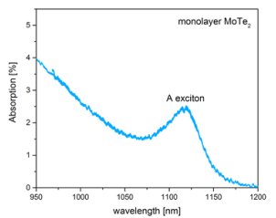
Figure 1: Absorption spectrum of monolayer MoTe2. The A exciton resonance is clearly visible at 1115 nm.
I. Niehues, R. Schmidt, S. Michaelis de Vasconcellos, R. Bratschitsch, University of Münster, Germany K. Unterrainer, Technische Universität Wien, Austria (December 2017)

© Oxford Instruments 2026
