Resources
 Part of the Oxford Instruments Group
Expand
Collapse
Part of the Oxford Instruments Group
Case Studies
Author: Dominik Bartl Robert, Bosch GmbH Corporate, Sector Research and Advance Engineering, Stuttgart
Published: 01 Oct 2013 · Last updated: 15 Jul 2025
Tags: ms-energy-app, libs-app
CIGS-based thin film solar modules are promising candidates for a cost-efficient conversion of solar energy into electricity. A thin film module consists of many single solar cells which are “monolithically interconnected” (see Fig. 1). This interconnection is achieved by selectively removing layers in 10 –100 µm wide grooves along the module during the production process. Small grooves (or “scribes”), which allow the electrical interconnection are created with a laser. However, it is important to make sure the laser only removes the material to a certain depth without damaging underlying layers, e.g. the conducting Mo film.
Plasma emission induced by the laser process can be used to identify the ablated material in order to control the “depth” of the laser scribe. This is possible because every layer of the solar cell has a different composition and thus different characteristic radiation is emitted depending on the ablated layer.
In this fundamental study we demonstrate the capability of our setup for the identification of single layers using the characteristic plasma emission of the elements contained in our layers. Furthermore we identify a suitable wavelength range for this analysis.
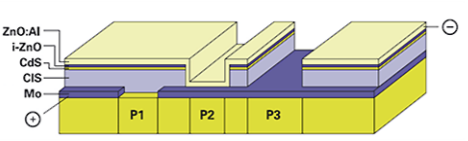
Fig. 1: Interconnection zone of thin film solar cells. The Mo forms the back electrode (+) and the ZnO:Al the front electrode (–) of the solar cell, respectively. Front and back electrode are electrically connected via the “P2” scribe
Our samples consist of a layer stack of 50 nm CdS, 50 nm ZnO, ~1.5 µm CIGS and ~400 nm Mo. This stack is deposited on a 3 mm thick soda lime glass sample (SLG, refer to Fig. 2).
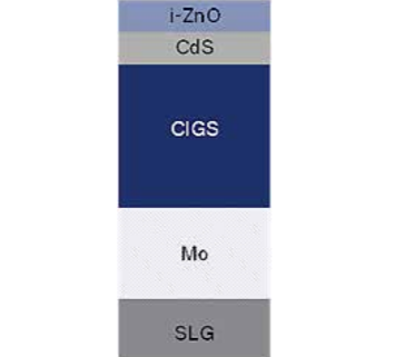
Fig. 2: Thin film sample consisting of a 50 nm thin ZnO layer, a 50 nm CdS layer, a 1.5 µm CIGS layer, and an approx. 400 nm thin Mo layer deposited on a soda lime glass (SLG) sample
For ablating the single layers we use a laser system delivering ultrashort pulses (pulse duration <1 ps) of 1030 nm, 515 nm or 343 nm wavelength. The acquisition system consists of a Czerny-Turner type spectrograph (Andor Shamrock SR-500i-B1) and an ICCD detector (Andor USB iStar DH340T-18U-E3). The ablation area (where the plasma forms) is imaged by means of a focusing mirror (see Fig. 3) onto one end of an optical fibre. The other end of the optical fibre is connected to the spectrograph and forms the entrance “slit”.
In order to determine and adjust the time delay between the laser pulse and the gate activation (“gate opening”) we use an oscilloscope to monitor the signal of a fast photodiode inside the laser and the electronic signal of the MCP (micro channel plate). A CNC-based positioning system is used for sample positioning.
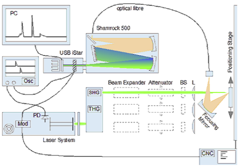
Fig. 3: Setup of acquisition system consisting of an ultrafast laser system (wavelength l = 1030 nm with second/third harmonic generation (SHG/ THG) for wavelength conversion to 515 nm and 343 nm), the shamrock spectrograph, an oscilloscope for delay adjustment and a CNC-based sample positioning system.
We first show fundamental tests, where we applied single laser pulses at the same position on the sample and acquired the corresponding spectrum of each laser shot. After a defined number of applied pulses we measured the ablated depth using a confocal laser scanning microscope. Fig. 4 shows the obtained spectra depending of the ablated depth of the sample. Please note that each spectrum shown corresponds to a certain ablated depth and therefore to a different number of pulses applied onto the same position of the sample. All layers of our sample are resolved in Fig. 4, including even the 50 nm thin ZnO and CdS layers, respectively, by observing the characteristic lines of the different elements.
Thanks to its many spectral lines the Mo can be easily recognized. Therefore, it is possible to control the depth of the laser scribed groove by monitoring specific spectral lines. In addition LIBS can be used for sample diagnostics.
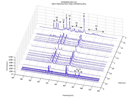
Fig. 4: Acquired spectra in single shot mode vs. ablated depth of the sample. The corresponding spectral lines of Zn, Cd, Mo, Ga and In are highlighted

© Oxford Instruments 2026
