Resources
 Part of the Oxford Instruments Group
Expand
Collapse
Part of the Oxford Instruments Group
Application Notes
Author: J. Martin, A. Weiß, Fraunhofer Institute for Electronic Nano Systems ENAS, Chemnitz
Published: 01 Feb 2012 · Last updated: 28 May 2026
Semiconductor nanocrystals are very promising materials for micro and nano systems integration. They offer several advantages compared to organic light emitters, among them excellent chemical stability and narrow emission bands. However nanocrystals are important not only for light emitting purposes, but also for nanosensing applications, using their sensitivity with respect to electrical fields and charges. Here we present some results on the characterization of the photoluminescence of cadmium selenide nanocrystals with respect to externally applied voltages.
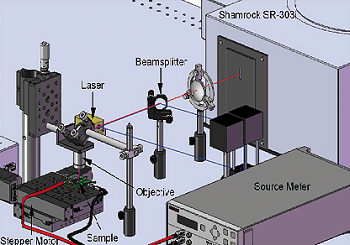
Figure 1. Schematic view of the confocal micro-spectroscopy setup.
In recent decades semiconductor nanocrystals, so-called 'quantum dots', have gained increasing attention for various applications such as fluorescent markers for cell imaging, and light emitting devices or detectors. Quantum dots show several advantages compared to organic light emitters. These are
This is a large benefit for integration of these emitters into micro systems since incompatibilities between different organic materials can be avoided. On the other hand, nanocrystals are very sensitive to electrical fields and charges, making them attractive for nanosensing applications.
Charges can be created inside the nanocrystals by Auger autoionization, or injected from outside the particle. The additional delocalized charge inside the core of a quantum dot leads in both cases to a non-radiative recombination of excitons. Hence a complete suppression of light emission from the respective ionized particle occurs, which can be observed as time-dependent photoluminescence bleaching of quantum dot ensembles. Based on this effect we are currently developing material for integrated sensors for large area detection, storage and visualization of mechanical overloads for lightweight structures.
The samples for charge injection experiments consist of several layers on ITO-coated glass substrates. These layers are necessary to ensure the correct energy levels for charge injection into the semiconductor quantum dots. CdSe/ZnS core/shell quantum dots with a nominal emission wavelength of 610 nm were embedded in a PMMA matrix to enhance the storage conditions for electrical charges inside the nanocrystals.
The layers are stacked in the following sequence from bottom: ITO anode, hole transport layer (N,N′-Bis(3- methylphenyl)-N,N′-diphenylbenzidine, TPD), nanocrystal-polymer composite, sputtered aluminum cathode. Preparation of the hole transport and the composite layer was done by spin-coating. The thickness of each layer is around 100 nm. All chemicals have been obtained from Sigma Aldrich.
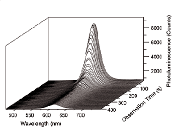
Figure 2. Series of photoluminescence spectra of CdSe/ZnS nanocrystals.
The optical characterization of the samples was done by means of time-resolved confocal micro-spectroscopy. Fluorescence properties were measured with a homebuilt setup (see Figure 1) based on a triple grating monochromator (Andor Shamrock SR-303i-A) with attached CCD (ANDOR Newton DU920P-BR-DD). Quantum dot photoluminescence was excited by a solid state laser at 475 nm wavelength (B&WTek Inc.), collected by a 63x, 0.75 N. A. Zeiss objective and imaged onto the entrance slit of the monochromator.
Electrical characterization was carried out using a source meter (model 2410, Keithley Instruments Inc.). Samples were analyzed by applying a voltage ramp with a slope of 0.5 volts per second. Each second, the sample current was measured and a photoluminescence spectrum was recorded. The combined electrooptical setup enables the correlation of current/voltage with the fluorescence signal of the quantum dots.
Using the described confocal setup, the photoluminescence of CdSe/ZnS quantum dots has been investigated during application of an external voltage across the composite layer. The applied voltage has been scanned from 0 to 41 volts for 82 seconds and kept constant at this level for additional 318 seconds while the photoluminescence was recorded simultaneously. A typical series of the quantum dot photoluminescence spectra is shown in Figure 2.
First the nanocrystal fluorescence stays roughly constant until a voltage of 20 V is reached. Then with increasing voltage the luminescence of the sample decreased steadily. We attribute this effect to an efficient charge injection into the particles.
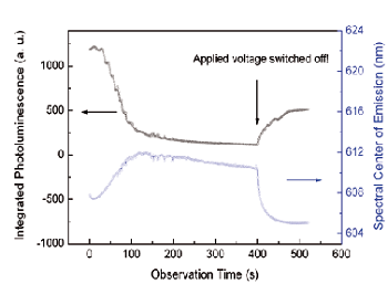
Figure 3. Time evolution of integrated quantum dot fluorescence and spectral shift.
Generally fluorescence reduction is attributed to the presence of a delocalized charge inside the nanocrystal. This charge in the respective particle leads to a non-radiative recombination of subsequent generated excitons and thus to an effective fluorescence suppression. But it is necessary to state, that according to the above-mentioned mechanism only one kind of charges, electrons or holes, may be injected into the particles. Obviously, this condition is nicely demonstrated with the selected materials and layer design.
The effect of the externally applied voltage on the nanocrystal fluorescence is evaluated in more detail in Figure 3. Here a trace of the integrated fluorescence is displayed with the spectral centre of the quantum dot emission band. Both signals are quite well correlated. The nanocrystal emission shifts steadily towards the red spectral range with decreasing intensity. Gradually more and more particles get ionized, while some nanocrystals remain neutral and emit photons continuously. The recombining excitons are affected by the electrical field of charged particles in the surroundings, resulting in a spectral shift to the red due to the Stark effect.
After 400 seconds observation time the applied voltage was switched off and the quantum dot fluorescence was recorded for another 120 seconds. The photoluminescence recovers immediately to some extent and the spectral shift is diminished as well. Both observations suggest a rather fast ‘escape’ of charges out of ionized particles, at least for a certain portion of the quantum dot ensemble. Recent measurements have shown that the polymer matrix plays a crucial role with respect to storage conditions and resulting storage time. Currently sample design is refined steadily to achieve higher optical contrast ratios and longer storage times.
Conclusion
We presented results on the investigation of the influence of electrical charges and fields on the photoluminescence of semiconductor nanocrystals. Due to their sensitivity to charge they are potentially useful for sensor applications. With PMMA as host material for the quantum dots an optical contrast ratio between the bright and dark state of roughly 1:10 has been achieved. A spectral red shift of the emission due to charging of the composite layer has been determined, in combination with photoluminescence reduction. Additionally, a fluorescence recovery after switching off the applied external voltage was detected. By extrapolating the fluorescence signal, we can estimate a time of several hours until the original intensity value is reached.

© Oxford Instruments 2026
