Resources
 Part of the Oxford Instruments Group
Expand
Collapse
Part of the Oxford Instruments Group
Application Notes
Author: R. Schmidt, R. Schneider, I. Niehues, S. Michaelis de Vasconcellos, R. Bratschitsch, Institute of Physics and Center for Nanotechnology, University of Münster
Published: 01 Nov 2016 · Last updated: 16 Jul 2025
Tags: ms-semiconductors-app, absorption-app
Monolayers of transition metal dichalcogenides, such as MoS2, MoSe2, MoTe2, WS2, WSe2, represent a new class of two-dimensional semiconductors. Their optical band gap in the visible and infrared regime renders them promising for optical and opto-electronic devices.
One of the most striking features of these materials are strong excitonic resonances with exceptional high binding energies on the order of hundreds of meV. Here, we investigate how these resonances can be manipulated by applying uniaxial strain to monolayers of WSe2 in a controlled and reversible manner. Using white light transmission spectroscopy, we measure the absorption of the A, B, C and D excitonic resonances of the monolayers, depending on the applied tensile strain.
To apply uniaxial, tensile strain, a monolayer of WSe2 is mechanically exfoliated on a flexible polycarbonate substrate and covered with a polymer layer (PDMS) (Figure 1a). By bending the substrate, the top surface expands, which causes straining of the attached WSe2 monolayer. The PDMS layer prevents the flake from slipping. With this configuration it is possible to reversibly apply a tensile strain of up to 1.5% to the monolayer.
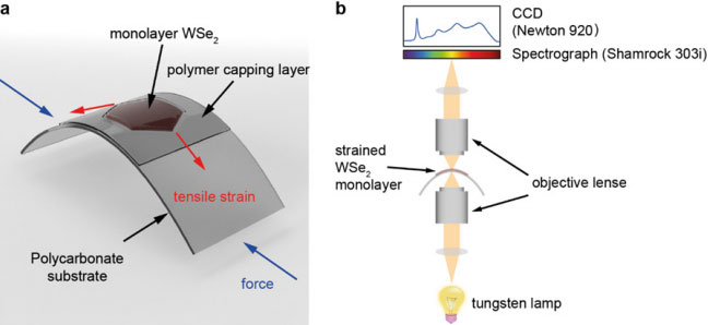
Figure 1. a) Illustration of the sample geometry. By bending the polycarbonate substrate, the monolayer on top can be reversibly strained. Figure 1. b) Schematic drawing of the transmission microscopy setup for the measurement of the strain dependent absorption of monolayer WSe2.
To measure the strain-dependent absorption spectra, we use a homebuilt transmission microscope setup (Figure 1b). The white light continuum from a tungsten halogen lamp is focused on the sample using an objective lens (50x/ NA=0.55) and illuminates an area in the sample plane. The transmitted light is collected by an objective lens (50x/ NA=0.6) and imaged on the entrance slit of an imaging spectrograph (Andor Shamrock SR-303i-B-SIL) with an attached CCD camera (Andor Newton DU920P-OE). By opening the entrance slit of the spectrograph and using a diffraction grating in zero order, an image of the sample is recorded by the CCD. Due to the high readout speed and frame rate of the Newton camera, the monolayer can be easily located. By closing the entrance slit and using the grating in first order, transmission spectra of the monolayer are projected to the horizontal axis of the CCD. In the vertical direction, transmission spectra along to the entrance slit can be simultaneously measured (green line in Figure 2a).
The optical absorption of the WSe2 monolayer is determined by measuring the light from the tungsten lamp transmitted through the sample TML compared to the light transmitted through the bare substrate TSubs. The absorption is then calculated by:

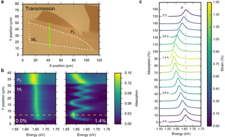
Figure 2a) Optical microscopy image in transmission of the WSe2 monolayer (dashed white line). Figure 2b) Spatially resolved transmission spectra (A exciton) for 0.0% and 1.4 % strain measured along the green line marked in a. Figure 2c) Absorption spectra for increasing and decreasing strain levels measured at the position of the yellow dashed lines in b. The spectra are vertically shifted for clarity.
Figure 2 shows an optical image of the WSe2 monolayer (a) and the measured absorption spectra (b and c). Due to the large size of the flake we are able to spatially resolve the absorption spectra across the monolayer. In the case of no applied strain shown (Fig. 2b), the A exciton is located at 1.66 eV everywhere on the WSe2 monolayer. If we increase the strain, the A exciton shifts to lower energies. However, this shift only occurs in the center of the flake, whereas it is zero at the edges. For even higher values of strain up to 1.4% the monolayer breaks, forming cracks perpendicular to the direction of the applied force. These cracks lead to an inhomogeneous distribution of the transferred strain to the monolayer, which causes prominent differences in the spatially resolved absorption spectra. In the center of the WSe2 monolayer some areas are visible, where the A exciton position is the same as for the unstrained case, and some areas, where the strain is transferred, i.e. the A exciton is at 1.58 eV. Obviously, the size of the monolayer is important for achieving the maximum strain transfer.
In conclusion, we found a shift of 71 meV to lower energies of the A exciton for an applied uniaxial tensile strain of 1.4% for WSe2 monolayers. The Andor Newton DU920P-OE camera allowed us to measure also spatially resolved transmission spectra of WSe2 monolayers over a wide energy range with a high framerate. We examined the spatial strain distribution in the WSe2 monolayer and found that the size of the monolayer was crucial for an efficient transfer of strain from the substrate to the monolayer. The camera can also be used for investigating other atomically thin materials, because it is sensitive down to 200 nm due to the open electrode configuration and shows no etaloning at longer wavelengths.
Appreciation is gratefully extended to Robert Schneider and Prof. Dr. Rudolf Bratschitsch, Institute of Physics and Center for Nanotechnology, University of Münster.

© Oxford Instruments 2026
