Resources
 Part of the Oxford Instruments Group
Expand
Collapse
Part of the Oxford Instruments Group
Application Notes
Author: A. Koitmäe, R. H. Blick, Center for Hybrid Nanostructures, Institute of Nanostructure and Solid State Physics, University of Hamburg
Published: 01 May 2015 · Last updated: 16 Jul 2025
The fabrication of the semiconductor microtubes is based on the principle of self-organized rolling-up of strained layers. [1] By tuning the layer thicknesses and compounds the diameter and band gap can be tuned to a desirable range. We fabricated microtubes of a length of 50 µm and a diameter of 3 µm including a quantum well emitting light in the near infrared regime. For the purposes of emitting light at a certain wavelength quantum well is embedded between two barrier layers in the subsequent layers (Fig.1).
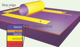
Fig. 1. The microtubes are fabricated via lithography by defining starting edges, stop edges and shallow mesa.
Photoluminescence measurements are mostly performed at low temperatures because of the advantages such as higher emission intensity and low exciton-phonon interaction resulting in low FWHM values. In terms of fundamental research such conditions are essential to have precise conditions, however room temperature characteristics play an important role for the industry to apply such systems in commonly used technical devices.
To excite the electrons from the valence to the conduction band, a green laser (552 nm) is used. The reflected beam coming from the confocal microscope is focused with a lens and directed into the spectrometer via mirrors (Fig.2).
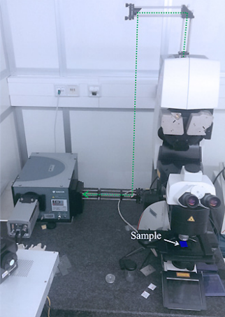
Fig. 2. The microtubes are excited via a green laser coming from the confocal microscope. The reflected beam is guided into the spectrometer where the emission spectrum of the microtube is detected.
The green dashed line shows the beam path from the confocal microscope to the spectrometer. The PL measurements were recorded using a Shamrock SR-303i-ASIL spectrograph with silver coated mirrors and gratings equipped with a Newton DU920P-BR-DD infrared sensitive CCD detector.
Fig. 3 shows emission characteristics of a 4 nm InGaAs quantum well at room temperature. The red curve refers to the emission of the quantum well showing peaks at 955 nm and 978 nm. A reference signal coming from the substrate (GaAs) is collected (black curve).
As expected, it shows no characteristic peaks in the shown region, but has a clear increase at around 820 nm (not shown) which is indicative to bulk GaAs. The double-peak phenomenon at room temperature was also observed by Dawson et.al.[2] However their measurements show a clear decrease of the highenergy tail of the spectrum. We detect this aspect on microtubes transferred from the GaAs wafer to a glass substrate coated with PDMS [3]. The emission spectrum of the microtube shows a characteristic peak at 814 nm which refers to the low-energy tail of the PL spectrum. The high-energy tail emits at 800 nm and shows a decrease in the intensity by a factor of 2.
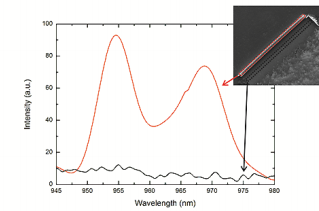
Fig. 3. Intensity plotted against the wavelength. The emission wavelength of a 4 nm InGaAs quantum well (red curve) has two peaks (955 nm and 968 nm). The black curve shows a reference measurement of the area next to the tube.
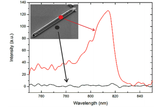
Fig.4. Intensity plotted against the wavelength. The emission curve of a transferred microtube on a glass/PDMS substrate with GaAs QW embedded in the tubes wall shows a characteristic peak at 814 nm (red curve, in comparison the glass/PDMS substrate shows no increase in this specific wavelength region (black curve).
In conclusion we have shown that the Newton CCD camera is sensitive enough to perform photoluminescence measurements of optically active semiconductor microtubes at room temperature.
[1] V. Y. Prinz, V. A. Seleznev, A. K. Gutakovsky, A. V. Chehovskiy, V. V. Preobrazhenskii, M. A. Putyato, and T. A. Gavrilova, “Free-standing and overgrown InGaAs/GaAs nanotubes, nanohelices and their arrays,” Physica E, vol. 6, pp. 828–831, 2000.
[2] P. Dawson, G. Duggan, H. I. Ralph, and K. Woodbridge, “Free excitons in room-temperature photoluminescence of GaAs-AlxGa1-xAs multiple quantum wells,” Phys. Rev. B, vol. 28, no. 12, pp. 7381– 7383, Dec. 1983.
[3] A. Koitmäe, C. S. Bausch, E. Stava, D. Sonnenberg, W. Hansen, and R. H. Blick, “Direct Transfer of GaAs Microtube Arrays onto Transparent Substrates for Imaging Neuron Outgrowth,” Soft Nanoscience Letters, vol. 3, pp. 79–82, 2013.

© Oxford Instruments 2026
