Resources
 Part of the Oxford Instruments Group
Expand
Collapse
Part of the Oxford Instruments Group
Application Notes
Author: Dr. Jörg Malindretos, Physikalisches Institut, Festkörper und Nanostrukturen, Georg-August-Universität Göttingen.
Published: 01 Oct 2020 · Last updated: 29 Nov 2022
Tags: ms-semiconductors-app, microspectroscopy-app, material-science-app
Since the beginning of the 1990s, the semiconductor GaN and its related compounds InN and AlN have taken a prominent position on the scene of semiconductor materials and devices. The successful p-type doping of the wide band gap semiconductor GaN opened the way to the development of efficient, robust and long-lasting blue light emitting diodes and laser diodes (LEDs and LDs). The impact on society was tremendous, leading to realization of ultra-high density optical data storage (Blue-ray Disc with a 405 nm wavelength LD) and most notably to “The invention of efficient blue light-emitting diodes which has enabled bright and energy-saving white light sources” (2014 Nobel Prize in Physics).
The growth of nanocolumns (NCs) is nowadays a well-known approach which is intensively studied also as a potential candidate for solid state lighting. Different facets (polar, non-polar and semi-polar) occur in GaN-based nanocolumns depending on the nanocolumn polarity. Control of the facets through the growth conditions might offer a further degree of freedom as compared to epitaxial layers. In particular, dense regular arrays of Ga-polar nanocolumns might serve as a template of semi-polar {1-10n} facets for the growth of InGaN/GaN multi quantum wells, which would not be affected by the strong polarization fields present along the polar directions. The latter cause a spatial separation of electron and holes in the InGaN/ GaN quantum-well active region, which increases with increasing indium content. This effect is detrimental for the development of high-efficient optical emitter in the longer wavelength range (green LEDs and LDs).
Selective area growth (SAG) by molecular beam epitaxy (MBE) is one possible choice for growing ordered GaN-based NCs, with a high degree of control. A thin Mo-layer (10-20 nm thickness) deposited on a GaN(0001)/sapphire template is patterned by electron beam lithography and subsequent dry etching, before insertion into the MBE growth chamber. The patterned areas consist of circular apertures in hexagonal arrangement. Several regular fields (80 x 80 µm2) have been designed with aperture diameters in the range between 50 nm and 500 nm and aperture pitches in the range between 0.25 µm and 8 µm and patterned in the central area of the substrate. In this way, MBE growth occurs under the same conditions of temperature and impinging fluxes and the mechanism of selective area growth can be studied as a function of the aperture array layout. Fig. 1 shows representative images of selective area growth of GaN nanocolumns which have been obtained in our group.
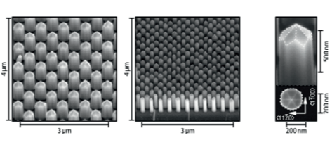
Fig. 1 – Bird’s eye view scanning electron microscopy (SEM) micrographs of SAG GaN nanocolumns with different NC diameters and aperture pitches (samples G1225 and G1253). To the right, bird’s eye view and top-view SEM micrographs of the typical pyramidal tip morphology, which corresponds to semipolar GaN surfaces. (Arne Urban, UGOE Dissertation 2013).
Micro-photoluminescence (µ-PL) measurements are a versatile tool for the characterization of the optical emission properties of individual nanowires and NC arrays. A confocal µ-PL setup has been realized using an Andor Shamrock 303i-A spectrograph and an Andor Newton DU920P-EX2-DD CCD detector. As the emission of GaN/InGaN ranges from the UV up to the entire visible spectrum, a back illuminated, deep depletion detector with extended range dual anti-reflection coating has been selected (BEX2-DD). This model exhibits broadband high quantum efficiency and shows only very little etaloning.
A schematic of the complete setup is shown in Fig. 2. A HeCd laser emitting at 325 nm is reflected off a dichroic mirror and focused onto the sample by a Thorlabs LMU-20X-NUV 20x microscope objective with a numerical aperture of NA=0.4. The sample is mounted inside an Oxford Microstat HiRes2 helium flow cryostat that offers precise temperature control from 3.2 K up to 500 K. Using two Thorlabs LNR50S/M linear translation stages driven by stepper motors, two-dimensional scanning is realized. This allows for the convenient measurement of photoluminescence maps. The luminescence emitted from the sample is collected by the same microscope objective and imaged onto a 20 µm confocal pinhole. From there, the signal is finally coupled into the Shamrock 303i spectrograph equipped with the Newton 920 CCD detector.
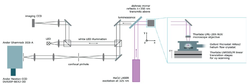
Fig. 2 – Schematic of the flexible and economical µ-PL setup for temperature dependent measurements in the UV-VIS spectral range.
The CCD chip can be cooled down to -80 ºC with air by means of a Peltier cooling stage. With additional water cooling of the Newton camera, the cooling can be reduced to about -100 ºC, which would further improve the signal-to-noise ratio and would allow for longer integration times. Additionally, the sample is imaged onto a second CCD using two beam splitters and a white LED for illumination. The setup is operated using the Micro-Manager open source microscopy software (µManager), which supports both, the Shamrock spectrograph via a plug-in provided by Andor, as well as the employed Thorlabs scanning stages.
A typical micro-photoluminescence mapping of a GaN NC array is demonstrated in Fig. 3. The integrated PL intensity map is shown in the left panel. The position of the individual NCs with a diameter of 500 nm and a pitch of 4 µm on a hexagonal 2D arrangement is clearly recognized. The overall PL intensity reveals inhomogeneities within the NC ensemble. The µ-PL spectra of individual GaN NCs are characterized by a dominant near-band-edge emission (NBE) at 3.458 eV (358.6 nm) (Fig. 3, right panel). However, the presence of additional emission at higher wavelength points to the presence of defects, in particular basal plane stacking faults (BSFs) that can be induced in MBE grown GaN NC arrays, as reported e.g. in our work [A. Urban et al., Nano Lett. 15, pp. 5105–5109 (2015)]. There the BSF emission is found in the range between 361 nm and 380 nm.
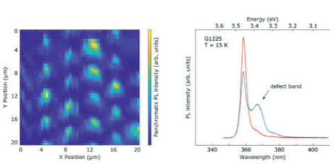
Fig. 3 – Low temperature micro-photoluminescence mapping of a GaN NC array (left). Two representative PL spectra of NCs with and without noticeable defect emission – most likely due to the presence of basal plane stacking faults (right).
In summary, a µ-PL setup for temperature dependent measurements in the UV-VIS spectral range has been devised and employed for the investigation of GaN nanocolumn arrays grown by molecular beam epitaxy.
J. Malindretos, C. Hilbrunner, A. Rizzi, IV. Physikalisches Institut, Festkörper und Nanostrukturen, Georg-August-Universität Göttingen, Germany (April 2019)

© Oxford Instruments 2026
