Resources
 Part of the Oxford Instruments Group
Expand
Collapse
Part of the Oxford Instruments Group
Application Notes
Author: Dr. Markus Clark Scharber, Linz Institute of Organic Solar Cells, Johannes Kepler University Linz
Published: 01 Jan 2019 · Last updated: 16 Jul 2025
Tags: ms-energy-app, material-science-app
The class of organic-inorganic halide perovskite semiconductors has attracted a lot of attention due to their outstanding optical and electrical properties. High performance photovoltaic devices (PVs) with excellent power conversion efficiencies (>22 %) and high performance light emitting diodes (LEDs) have been reported recently. However, the physics and chemistry of organic-inorganic halide perovskite semiconductors and related devices are not well understood. For solar cells and LEDs radiative recombination is the most important ingredient for high performance. Therefore, a detailed understanding of photon absorption and recombination of photo-excited states in perovskite materials is important to study the quality and potential of synthesized materials.
Perovskite layers with the chemical composition CH3NH3PbI3 are deposited on sapphire substrates from solution. Process details are described in [1]. Samples are attached to a copper holder and mounted on the cold finger of a closed-cycle helium cryostat. A pulsed, frequency-doubled Nd-YAG laser (Innolas SpitLight Compact 100, 10 Hz) is applied as excitation source. The pulse energy is adjusted with neutral density filters to achieve 0.1 mJ/cm2 at the sample position. The sample emission is collected with a lens and guided to the detection unit with an optical fiber. A long pass filter (550 nm) removes the excitation light before the collected radiation is fed into a monochromator (Andor Shamrock 303i, grating 500 nm blaze, 150 lines/mm) and detected with an intensified charge-coupled device (Andor iStar DH320T-18U-73). Spectra are recorded with 2.5 ns gate width and 2.5 ns gate step. A sketch of the experimental setup is shown in Figure 1.
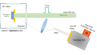
Figure 1: Experimental setup
Figure 2 shows the photoluminescence spectra recorded at different delay times. The emission intensity increases at lower temperatures. At 125 K the emission shifts to higher energies and the peak splits into two features.
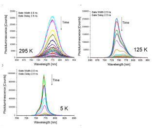
Figure 2: Photoluminescence spectra of a MAPbI3 film recorded after different delays and different temperatures.
Analyzing the decay kinetics is very challenging due to complicated line-shapes and several different decay times can be extracted from the recorded spectra. Figure 3 shows integrals of individual spectra at 5 K, 125 K and 295 K versus time.
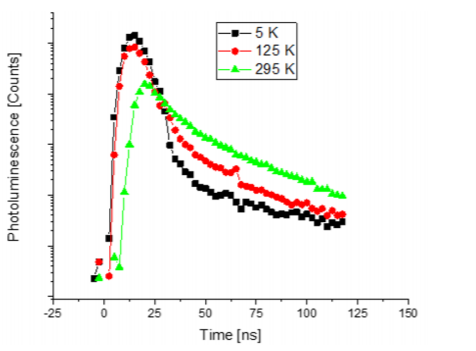
Figure 3: Photoluminescence kinetics of a MAPbI3 sample recorded at different temperatures.
All spectra show at least one short-lived and one longlived component and the decay appears to be faster at low temperatures.
In this application note photoluminescence experiments on thin perovskite layers are described. We find that this perovskite semiconductor exhibits a complicated temperature dependence of the PL spectra suggesting that the system undergoes various phase transitions. The applied experimental arrangement is ideal for the performed experiments as the spectral and the timedomain kinetics can be studied at the same time.
[1] Adam, G., et al. (2016). Solar Energy Materials & Solar Cells Solution processed perovskite solar cells using highly conductive PEDOT : PSS interfacial layer, 157, 318. doi.org/10.1016/j. solmat.2016.05.011.

© Oxford Instruments 2026
