Resources
 Part of the Oxford Instruments Group
Expand
Collapse
Part of the Oxford Instruments Group
Application Notes
Author: Philipp Tonndorf & Prof. Dr. Rudolf Bratschitsch, Institute of Physics and Center for Nanotechnology, University of Münster.
Published: 01 Dec 2015 · Last updated: 16 Jul 2025
Tags: ms-quantum-app
Monolayers of transition metal dichalcogenides (TMDCs), such as MoS2, MoSe2, WSe2, and WSe2 are promising for conceptually new opto-electronic devices. These TMDCs are direct band gap semiconductors and exhibit valleytronic effects. Recently, transistors, photodetectors, and light emitting devices have been demonstrated using these materials. Here, we present single-photon emission of localized excitons in monolayer WSe2 [1], which suggests that TMDCs are also promising for quantum optics.
WSe2 monolayers are obtained by mechanical exfoliation of a bulk single crystal [2]. The photon emission from the atomically thin layers is investigated in a homebuilt laser scanning confocal microscope with a deep depletion CCD (Andor iDus DU420A-BR-DD) attached to spectrograph (Andor Shamrock SR-750-D1- SIL). For excitation, either a 532 nm diode-pumped solid state laser or a tunable Ti:Sapphire laser are used.
Fig. 1 shows a photoluminescence map of the WSe2 monolayer at a temperature of 10 K. The laser is scanned over the sample and at each point the spectrum is recorded. In Fig. 1a) the broad energy range of 1.55 – 1.77 eV is shown. The monolayer is clearly visible with some bright emission centres at the edges of the flake. Photoluminescence spectra recorded from different positions (i-v) are depicted in Fig. 1b. The typical photoluminescence emission of the WSe2 monolayer (position v) exhibits two maxima due to the neutral exciton (X0 at 1.747 eV) and charged exciton (X± at 1.718 eV), together with a broad emission band at lower energies. At the bright centre positions at the flake edges, sharp emission lines are found (i-iv). The second-order correlation function measured with a Hanbury-Brown and Twiss setup proves that the localized emitters are excellent single-photon sources [1].
Photoluminescence in the narrow energy window around 1.694 eV containing some of these centres is shown in Fig. 1c. The photon emission at energy of the free neutral exciton (1.745 eV) is plotted in Fig. 1d. It is clearly visible that at the positions of the bright emission centres the intensity of the free neutral exciton X0 is strongly decreased. This observation together with evidence from photoluminescence excitation spectroscopy suggest that the single-photon emitters are originating from localized excitons.
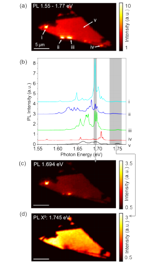
Figure 1. Photoluminescence mapping of a WSe2 monolayer with localized emission centers. a) Broad spectral range from 1.55 to 1.77 eV. b) Spectra for positions i-v. c), d) Narrow spectral range. The grey rectangles indicate the spectral window used in (c) and (d).
The spectrum in Fig. 2 obtained with a high resolution grating (1800 lines/mm) reveals that the spectral width of the emission lines of centres in freestanding WSe2 monolayers is less than 120 µeV, which is the spectral resolution of the system. Due to the high detection efficiency of the iDus CCD the spectral wandering of the two emission lines can be measured with 0.1 s time resolution (Fig. 2b). We used a spectral diffusion of 500 µeV over 8 minutes.
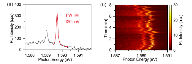
Figure 2. Photoluminescence spectrum of localized excitons. a) High resolution spectrum with 1800 lines/mm grating. b) Spectral diffusion over 8 minutes.
With the help of the Andor iDus 420 CCD camera attached to a Shamrock 750 spectrograph we have characterized single-photon emitters in atomically thin WSe2.
[1] P. Tonndorf, R. Schmidt, R. Schneider, J. Kern, M. Buscema, G. A. Steele, A. Castellanos-Gomez, H. S. J. van der Zant, S. Michaelis de Vasconcellos, R. Bratschitsch, Optica 2, 347-352 (2015).
[2] P. Tonndorf, R. Schmidt, P. Böttger, X. Zhang, J. Börner, A. Liebig, M. Albrecht, C. Kloc, O. Gordan, D. R. T. Zahn, S. M. de Vasconcellos, R. Bratschit

© Oxford Instruments 2026
