Resources
 Part of the Oxford Instruments Group
Expand
Collapse
Part of the Oxford Instruments Group
Technical Article
Author: Tom Seccull
Published: 01 Nov 2025 · Last updated: 19 Nov 2025
Achieving high frame rates and minimising data transfer latency is necessary in many experiments and instruments that incorporate scientific imaging cameras. Frame rate is the speed at which consecutive images can be continuously acquired. Data latency is the speed at which imaging data can be read off the camera head into a computer’s memory for storage or immediate processing. Frame rate and latency are related, such that optimising a camera for one may readily lead to improvements in the other, but there are cases where either may be prioritised in the camera’s operation. Use of Fast Kinetics mode to image rapidly evolving quantum gases exemplifies an application where frame rate is more important than data latency [e.g. 1]. Ion trap quantum computers must coordinate multiple complex optical, electrical, and mechanical systems with nanosecond precision based on images of the quantum states of trapped ion qubits. In this case, minimising data latency often takes priority over absolute frame rate in the race to coordinate, process, and read qubits before quantum decoherence occurs [e.g. 2,3]. Adaptive optics systems designed to measure and compensate for rapidly varying image distortions caused by atmospheric turbulence are an example of an application requiring both high frame rates and minimal latency [e.g. 4].
This note provides a visual guide and summary of how operating Andor’s Charge Coupled Device (CCD) and Electron-Multiplied Charge Coupled Device (EMCCD) cameras in different ways affects both their achievable frame rates and the latency of their data readout and transfer. Figures presenting the peak frame rates achievable by each camera under different operating conditions are presented and overall trends revealed by the data are identified to help clarify how a camera’s performance is affected by the way it’s used.
Disclaimer: The figures presented for each camera in this note have been produced with the frame rate data provided in their publicly available spec sheets. The data in the spec sheets have been experimentally measured by Andor and provide a representative quantification of each camera’s performance. That said, it is not recommended to use these plots to predict a camera’s performance in parameter spaces where the data have been interpolated or extrapolated. This note focuses on the overall trends in the data (i.e. relative shape and position of each curve in the plots). For these purposes the absolute values of any given set of data points are less important. If you require absolute data about a camera’s performance with your specific experiment or instrument, we recommend that you contact us to request the loan of a demo camera with which to make your own measurements. Likewise, data latency is a complex parameter affected by multiple properties of both the camera and the system it is integrated with. True measurements of data latency for any given experiment or system are best obtained by demoing a camera in the field. Contact us if you are interested in learning more about this.
For what follows it’s helpful to briefly review the basic operation of cameras that use electron multiplied or standard CCDs as sensors. More detailed articles on this subject can be found on the Andor Learning Centre:
Most important to remember is that CCDs are serial readout devices. This means that any photoelectrons collected in the pixels of the sensor must be shifted (or clocked) across the array toward the shift register. Once in the shift register, the charges must then be clocked out of the sensor through the readout amplifier that measures the charge in each pixel and converts this signal to a voltage. Both the uncertainty of the amplifier’s measurement (read noise) and the pixel readout rate are proportional to the amplifier’s bandwidth. This means that precise measurement of the charge in each pixel is only achievable if pixel readout is performed relatively slowly.
Frame transfer CCDs have some of their area optically masked and dedicated to storage. Rather than having to wait for sensor readout to complete before starting the next frame, frame transfer CCDs can simply clock the recorded image from the image area of the sensor to the storage area where it can then be read out as normal. The time taken to vertically clock one pixel row into the storage area is typically on the order of microseconds (e.g. 0.6 µs for the iXon Ultra 888; 38 µs for the iKon-L). Clocking 1000 pixel rows into the storage area therefore takes on the order of milliseconds, which is a lot less than the 10 seconds needed to read out a conventional 1000x1000 CCD array at a standard low noise pixel read rate of 0.1 MHz. Note that the readout amplifiers of frame transfer CCDs are the same as those in standard CCDs and cannot read out an image quickly without increasing read noise. Shunting an image to a storage area for readout does, however, quickly free up the optically exposed part of the sensor to begin another exposure while a standard readout occurs in the masked region. As a result, frame transfer CCDs can achieve higher frame rates than standard CCDs.
EMCCDs are like standard CCDs in most respects apart from the addition of an electron multiplying shift register that facilitates the multiplication of charges in each pixel through impact ionisation. A small charge entering the multiplication register may exit the register multiplied by a factor of up to 1000. In comparison to the strength of the multiplied signal, the increase in read noise inherent to rapid pixel readout may be very small. This means that an EMCCD can read out images at a much higher rate than a typical CCD while maintaining relative measurement precision.
Once read off the sensor, image data is typically sent to the camera’s on-head memory and FPGA for some processing steps before transfer to a computer via one of the camera’s data interfaces.
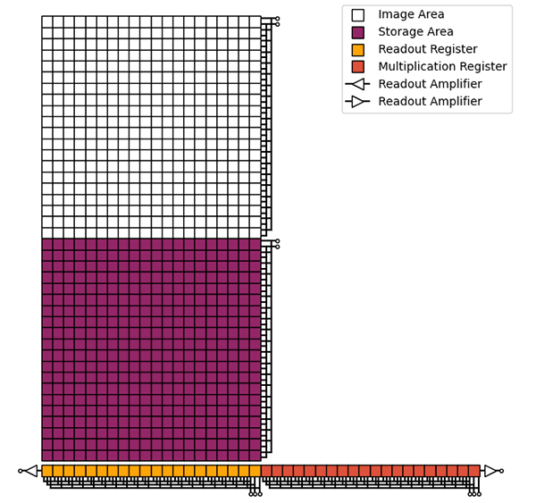
Figure 1 - Illustration of the structure of an EMCCD sensor that labels its different regions. Black lines and nodes attached to the pixels represent charge clocking circuitry.
Figure 1 illustrates the structure of a typical EMCCD sensor like those installed in Andor’s iXon range of EMCCD cameras. Highlighted sections include the image and storage areas of the sensor array, the readout register, the multiplication register, and two readout amplifiers. Most conventional CCD sensors lack a multiplication register and storage area but may still have multiple readout amplifiers to improve pixel read rates. Conventional frame transfer CCDs are less common and are comparatively expensive owing to the sacrifice of a large portion of their field of view to an optically masked storage section.
Figure 2 presents the structure of the EMCCD sensor installed in the OCAM2K and OCAM2S EMCCD cameras. OCAM is an EMCCD camera developed for wavefront sensing in high performance adaptive optics systems and is optimised for speed above all. Although the layout of this sensor is very different to that of the sensors used in the iXon, many of the same structures and components are present. Further details about this sensor will be described in this article as they become relevant.
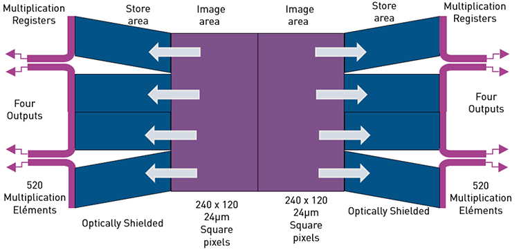
Figure 2 - Illustration of the structure of the CCD220 sensor installed in the OCAM EMCCD camera.
The following is a description of several ways in which the peak frame rate and latency of a CCD camera may be affected by the way it is used. This discussion will refer to Figures 3-6 in the following section that display frame rate data for the iKon-M 934, iKon-L 936, iKon-XL 230, and iKon-XL 231 CCD cameras . Figures 7 and 8 respectively present frame rate data for the iXon Ultra 888 and 897 EMCCD cameras. Remember that the frame rates presented in these plots account for the readout performance of the entire camera head under specific conditions. As a result, they are not generally applicable to all experimental setups or instruments. No plot is presented for the OCAM, but for reference this camera can reach a frame rate of 2067 frames per second (fps) under standard unbinned full frame operation. With 2x2 on-head pixel binning, OCAM is capable of 3625 fps full frame readout.
It should come as no surprise that it takes less time to read out and transfer smaller quantities of data. If allowable for a given experiment or system, there are multiple ways that the volume of data produced by a camera can be reduced to boost frame rates and reduce latency. Unlike some sCMOS cameras, (EM)CCD cameras do not typically have a configurable bit depth (16-bit digitisation is most common), so the two ways to impact data volume are to crop the size of the sensor’s Region of Interest or use on-chip pixel binning.
On-chip pixel binning sacrifices image resolution to improve readout speed. This is possible because pixel binning reduces the number of horizontal clocks and pixel reads respectively performed by the shift register and readout amplifier for each image readout (see this article for more details). The number of vertical clocks does not change, however, which results in diminishing improvements to readout speed as the degree of binning is increased. As shown in Figures 3-7, the greatest improvements to frame rate and latency are achieved with modest degrees of binning (e.g. going from unbinned to 2x2 binning).
Imaging with a small subarray of the full sensor as a Region of Interest (RoI) reduces the number of pixels that need to be read out per frame and may also reduce the total number of vertical and horizontal clocks needed to get image pixels to the readout amplifier. The trade-off here, of course, is reduced field of view.
Primarily used as a wavefront sensing camera, OCAM’s small sensor format (240x240 pixels; Figure 2) inherently records images with small data volumes that can be read out rapidly.
Further improvements to latency and frame rate can be realised if the distance between the RoI and the readout amplifier is minimised. Even though the times taken to read out one pixel or vertically clock a row are measured in units of microseconds, this time adds up quickly if an image is comprised of hundreds to thousands of rows each comprised of hundreds to thousands of pixels.
Andor CCD and EMCCD cameras provide configurable clocking and readout frequencies that are provided for reference in each camera’s spec sheet. Table 1 below summarises these details for popular models of Andor CCD and EMCCD camera at time of writing.
| Camera | Vertical Clock Speed, µs | Pixel Read Rate, MHz | Pixel Read Time, µs | Read Noise (No EM), e- |
| iXon Ultra 888 | 0.60 - 4.33 | 0.10 - 30.00 | 10.000 -0.033 | 3.5 - 130.0 |
| iXon Ultra 897 | 0.30 - 3.33 | 0.08 - 17.00 | 12.500 -0.059 | 2.7 - 89.0 |
| iKon-M 934 | 11.30 - 67.30 | 0.05 - 5.00 | 20.000 - 0.200 | 2.9 - 18.0 |
| iKon-M 934 DD | 4.25 - 64.25 | 0.05 - 5.00 | 20.000 -0.200 | 3.3 - 13.6 |
| iKon-L 936 | 38, 76 | 0.05 - 5.00 | 20.000 -0.200 | 2.9 - 31.5 |
| iKon-L 936 DD | 38, 76 | 0.05 - 5.00 | 20.000 -0.200 | 8.7 - 70.3 |
| iKon-XL 230 | 179.0 | 0.10 - 4.00 | 10.000 – 0.250 | 3.8 – 23.0 |
| iKon-XL 231 DD | 102.5 | 0.10 – 3.00 | 10.000 –0.333 | 2.1 – 9.8 |
Table 1 - Vertical clocking times and pixel read rates for a selection of Andor's CCD and EMCCD cameras. Camera models marked DD have deep depleted sensor variants. All read noise values are provided for conventional readout without electron multiplication (which could otherwise effectively negate read noise).
To minimise the number of vertical clocks and horizontal shifts required to read out an RoI from the sensor, the RoI can be placed in the corner of the sensor closest to the readout amplifier. Further improvements to frame rate and latency are possible when operating the camera in Crop Mode. In addition to tethering the RoI to the corner of the sensor nearest the readout node Crop Mode adjusts the sensor’s keep-clean cycles and clocking procedure such that it behaves like a sensor only as large as the RoI. In Crop Mode only the RoI is read and kept clean. This has the benefit of greatly improving the sensor’s speed, as it only needs to manage the RoI. On the other hand, Crop Mode requires the unused part of the sensor to be optically masked to ensure that scattered or background photons don’t cause counts to build up in pixels that aren’t being regularly read or cleaned. If left unmasked, pixels in the unused region may saturate and photoelectrons may spill into neighbouring pixels, potentially resulting in the presence of blooming artifacts in the images read from the RoI. The improved performance of Crop Mode over simple RoI corner-tethering is evident for Andor’s iXon Ultra EMCCD cameras when comparing the left two panels in both Figures 7 & 8.
In most optical systems, images formed on the optical axis have higher quality than those formed off-axis, which means a corner-tethered RoI may not provide the optical quality required for some experiments. For this reason, the iXon Ultra also provides an optically centred Crop Mode with multiple selectable RoIs. In most cases optically centred Crop Mode will not perform as well as corner tethered Crop Mode, but it still easily outpaces operating the camera with Crop Mode switched off (see Figs. 8 & 9).
Although only presented here for Andor’s iXon EMCCD cameras, Crop Mode is also provided with our iKon-M and iKon-L CCD cameras. Further details about Crop Mode can be found on the Andor Learning Centre:
A final important point when considering the effects of charge clocking distance on a camera’s frame rate and latency performance is the presence of the storage area on frame transfer CCD and EMCCD sensors. In all operating modes images must be clocked across the storage area to reach the shift register, and the size of the storage area typically matches that of the imaging area. It’s therefore worth considering this fact when choosing a camera with a frame transfer sensor, especially in experiments where image RoIs are very small and minimising latency is more important than maximising overall frame rate. Ion trap quantum computing experiments are an example of the kind of work that might occupy this operational parameter space. For large RoIs much of the readout latency is dominated by the time taken to read the pixels in each image. As RoIs get smaller, however, the latency contributed by clocking the image through the storage area becomes non-negligible. In these latter cases it’s worth considering the use of a smaller frame transfer sensor with a reduced distance between the imaging area of the sensor and shift register to minimise latency. For example, in this situation one might benefit by choosing the iXon Ultra 897 over the iXon Ultra 888.
Increasing the speed at which charges are vertically clocked toward the shift register may increase frame rates and decrease latency, with greater benefits when reading out small RoIs.
Andor’s iXon Ultra EMCCD cameras are capable of extremely fast sub-microsecond clocking which helps them to minimise Clock Induced Charge noise (particularly important in photon counting experiments). This extremely fast clocking increases the risk that charges may be left behind during readout, however, leading to the final image being distorted. One way to counter this smearing of charges is to carefully increase the clocking voltage to ensure that charges can be vertically clocked with both speed and accuracy. The clocking speed and voltage can be adjusted both with Andor’s Solis software and via the Andor SDK.
As presented by the curves plotted in Figures 3-7, one readily achievable way to improve frame rates and readout speed is to increase the camera’s pixel read rate. As discussed before, however, this comes at the cost of increased read noise. Read noise (measured in e-) is provided for each pixel read rate with data plotted in Figures 3-7. Note that each sensor has a slightly different performance at a given pixel read rate. Selection of a pixel read rate should be done carefully with consideration of the relative contributions of different noise sources to the overall noise in the final images. In some situations (e.g. high background shot noise) other noise sources may dominate to the extent that faster pixel read rates may be used without meaningful degradation of the final signal-to-noise ratio of the data.
Fast Kinetics mode (available with the iKon-M and iXon Ultra) takes advantage of the microsecond timescales typical for vertical clocking to make it possible to image small RoIs with a CCD at extremely high frame rates. This is only possible in short bursts though. The comparatively low pixel read rates of CCD sensors required to minimise read noise ultimately limit their ability to continuously sustain high frame rates.
Pixel read rate may be increased by simultaneously reading through more than one readout node. Andor’s large format CCD cameras, the iKon-XL 230 and iKon-XL 231, can be read out either through a single node, or simultaneously through four nodes. In four port readout mode, each readout amplifier reads the quadrant of the sensor that is nearest to it. Because each amplifier has slightly different read noise characteristics, it is important that any calibration frames (biases, flats, etc.) be read out in the same way to ensure accurate quantitative calibration of science images. Despite its small format (240x240 pixels), the EMCCD sensor in OCAM (Figure 2) is read out through eight separate nodes to maximise frame rate and minimise readout time.
In most normal use cases, CCD cameras will not produce data at high enough rates to warrant the use of a high-performance data interface. The versatile and widely used USB 2.0 or USB 3.0 interfaces are usually enough to handle the data stream and transfer images from the camera head to the user’s computer in a sufficiently short time. It’s recommended, however, that any CCD camera be connected to your computer via the dedicated USB controller card supplied with it. Doing this ensures the camera consistently operates at peak performance and won’t need to compete for resources with other devices connected to your motherboard’s bus.
Some demanding applications, like adaptive optics or ion trap quantum computing, where the camera forms an integral part of an optomechanical control feedback loop, require latency below what USB can provide. Andor’s iXon EMCCD cameras are provided with a low latency Camera Link data output to support direct data transfer from the sensor (bypassing the FPGA) on sub-millisecond timescales. Compared to USB, more of Camera Link’s bandwidth is dedicated to data transfer instead of handshaking communication protocols between the camera head and the computer, allowing larger volumes of data to be transmitted at higher speeds. iXon’s Camera Link interface is dedicated only to data downlink which means that camera control must still be performed through the normal USB interface. Camera Link is the only interface offered with OCAM.
Andor’s Learning Centre provides articles comparing data interfaces and describes the iXon’s Camera Link output interface in more detail:
The following plots graphically display the frame rate data from the spec sheets of some of Andor’s CCD and EMCCD cameras. Remember that the frame rates presented in these plots account for the readout performance of the entire camera head under specific conditions. As a result, they are not generally applicable to all experimental setups or instruments.
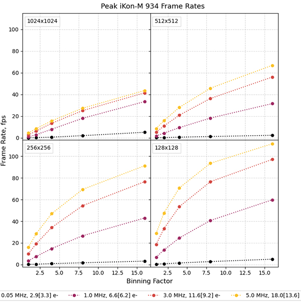
Figure 3 - Peak frame rates for the iKon-M 934 CCD Camera plotted against on-head pixel binning factor. Each panel shows the same for a sensor RoI with pixel dimensions labelled at the panel’s upper left corner. Available pixel read rates (in MHz) and the read noise (in e-) associated with each are colour coded as shown by the legend below the plots. Data for this plot were obtained from Andor’s iKon-M 934 spec sheet (version LiKonM934SS 0924 R1). As stated in that spec sheet, all measurements were made with the BEX2-DD variant of the iKon-M 934 and used a 4.25 µs vertical shift (clocking) speed with an assumption that the camera was operated with internal triggering and the exposure time.
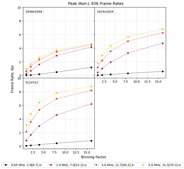
Figure 4 - Peak frame rates for the iKon-L 936 CCD Camera plotted against on-head pixel binning factor. Each panel shows the same for a sensor RoI with pixel dimensions labelled at the panel’s upper left corner. Available pixel read rates (in MHz) and the read noise (in e-) associated with each are colour coded as shown by the legend below the plots. Data for this plot were obtained from Andor’s iKon-L 936 spec sheet (version LiKonLSS 1124 R1). As stated in that spec sheet, all measurements used a 38 µs vertical shift (clocking) speed with an assumption that the camera was operated with internal triggering and the minimum exposure time.
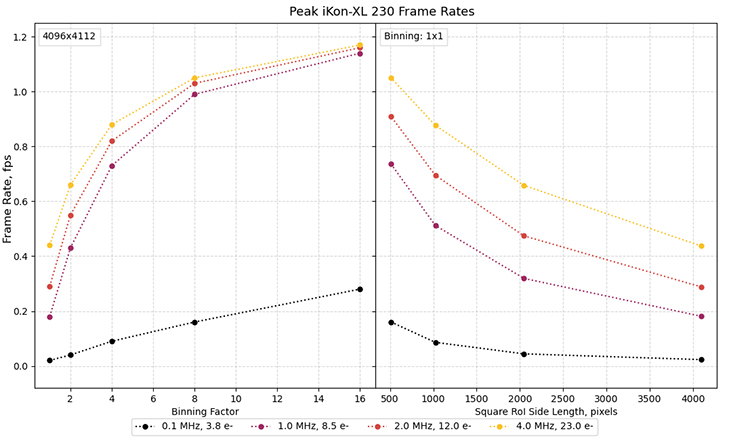
Figure 5 - Peak frame rates for the iKon-XL 230 CCD Camera plotted against on-head pixel binning factor (left panel) and RoI size assuming an RoI with a square shape. Available pixel read rates (in MHz) and the read noise (in e-) associated with each are colour coded as shown by the legend below the plots. Data for this plot were obtained from Andor’s iKon-XL 230 spec sheet (version iKonXL230SS 1224 R1). As stated in that spec sheet, all measurements used a 179 µs vertical shift (clocking) speed and all four available readout nodes. The camera is assumed to be operated with internal triggering and the minimum exposure time.
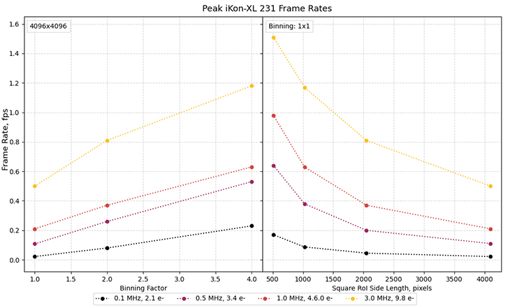
Figure 6 - Peak frame rates for the iKon-XL 231 CCD Camera plotted against on-head pixel binning factor (left panel) and RoI size assuming an RoI with a square shape. Available pixel read rates (in MHz) and the read noise (in e-) associated with each are colour coded as shown by the legend below the plots. Data for this plot were obtained from Andor’s iKon-XL 231 spec sheet (version iKonXL231SS 1224 R1). As stated in that spec sheet, all measurements used a 102.5 µs vertical shift (clocking) speed and all four available readout nodes. The camera is assumed to be operated with internal triggering and the minimum exposure time.
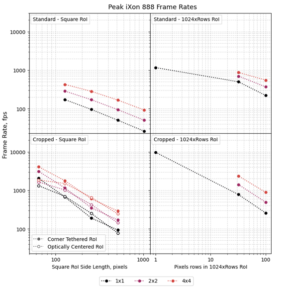
Figure 7 - Peak frame rates for the iXon Ultra 888 EMCCD Camera plotted against the dimensions of the RoIs being read out. On-head pixel binning factors for each data set are colour coded as shown by the legend below the plots. Data for this plot were obtained from Andor’s iXon Ultra spec sheet (version LiXonUltraSS 0425 R1). As stated in that spec sheet, all measurements used a 0.6 µs vertical clock speed and a 30 MHz pixel read rate. The camera is assumed to be operated with internal triggering. Solid points represent RoIs that are “corner tethered”, while empty points represent those that are “optically centred”.
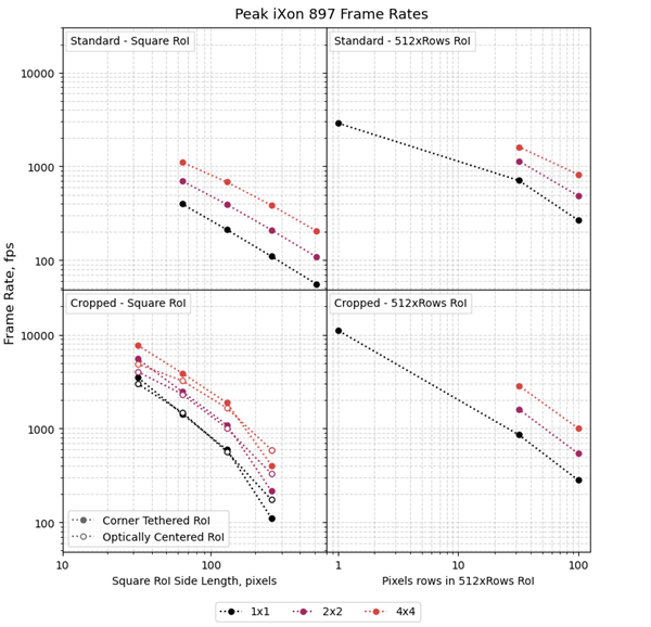
Figure 8 - Peak frame rates for the iXon Ultra 897 EMCCD Camera plotted against the dimensions of the RoIs being read out. On-head pixel binning factors for each data set are colour coded as shown by the legend below the plots. Data for this plot were obtained from Andor’s iXon Ultra spec sheet (version LiXonUltraSS 0425 R1). As stated in that spec sheet, all measurements used a 0.3 µs vertical clock speed and a 17 MHz pixel read rate. The camera is assumed to be operated with internal triggering. Solid points represent RoIs that are “corner tethered”, while empty points represent those that are “optically centred”.
References

© Oxford Instruments 2026
