Resources
 Part of the Oxford Instruments Group
Expand
Collapse
 Part of the Oxford Instruments Group
EMCCD technology, sometimes known as ‘on-chip multiplication’, is an innovative sensor technology first introduced to the digital scientific imaging community by Andor Technology in 2001, with the launch of the high-end iXon EMCCD Camera platform of ultra-sensitive cameras. Essentially, the EMCCD is an image sensor that is capable of detecting and quantifying single photon events without an image intensifier. This is made possible by way of a unique electron multiplying structure built into the chip. Over the years this technology has been refined resulting in the iXon Ultra and Life series that deliver sensitivity that remains unmatched.
EMCCD cameras overcome a fundamental physical constraint to deliver high sensitivity with high speed. Traditional CCD cameras offered high sensitivity, with readout noises in single figure range <10e- but this was only possible at the expense of slow readout. Hence, they were often referred to as ‘slow scan’ cameras. The fundamental constraint came from the CCD charge amplifier. To achieve a high-speed operation, the bandwidth of the charge amplifier needs to be as wide as possible, but the noise scales with the bandwidth of the amplifier, hence higher speed amplifiers have higher noise. Slow scan CCDs have relatively low bandwidth and hence can only be read out at modest speeds, typically less than 1MHz.
EMCCD cameras avoid this constraint by amplifying the charge signal before the charge amplifier and therefore can deliver unprecedented sensitivity at high speeds. Amplification of the signal prior to readout means that the readout noise is effectively bypassed, and the readout noise that normally sets the limit on sensitivity in CCD and CMOS is negated.
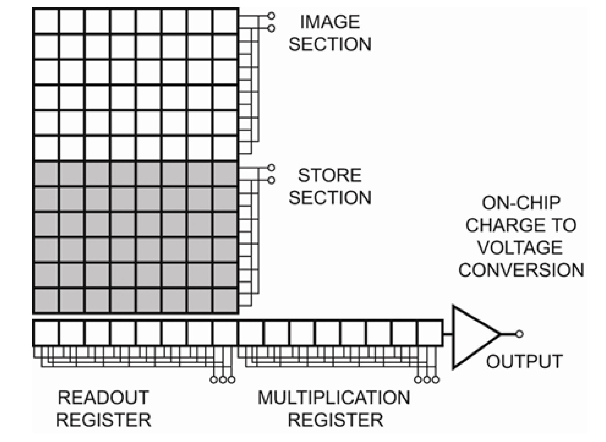
Figure 1: An illustration of the structure of the EMCCD sensor
Most EMCCDs also utilise a Frame Transfer CCD structure as shown Figure 1. Frame Transfer CCDs feature two areas – the normal sensor “image section” which captures the image and an additional “storage area”, where the image is stored prior to read out. The storage area is typically identical in size to the sensor area and is covered with an opaque mask, normally made of aluminium. During an acquisition, the sensor area is exposed to the light signal and an image is captured, this image is then automatically shifted downwards behind the masked region of the chip, and then read out. While this is happening, the sensor area is ready to gather the signal for the next image. The aluminium mask of the Storage section of the sensor therefore acts like an electronic shutter or buffer. To readout the sensor the charge is shifted out through the readout register and then through the multiplication register. It is here in the multiplication register that the amplification process of the EMCCD camera occurs prior to the final readout by the charge amplifier.
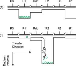
Figure 2: The Gain register of the EMCCD features many hundreds of cells that exploit impact ionization under the presence of an electric potential.
The amplification occurs in the multiplication register through the scheme highlighted in Figure 2. The multiplication register of an EMCCD camera contains many hundreds of cells and the amplification process occurs in each cell by harnessing a process which occurs naturally in CCDs known as Clock-Induced Charge (also called Spurious Charge). Clock-induced charge has traditionally been considered in a negative sense as a source of noise, and something to minimise, but not for EMCCDs. When “clocking” the charge through a register there is a very tiny but finite probability that the charges being clocked can create additional charges by a process known as ‘impact ionization’. Impact ionization occurs when a charge has sufficient energy to create another electron-hole pair and hence a free electron charge in the conduction band can create another charge. It is from this that amplification of even a very small signal is possible.
To make this process viable, EMCCDs control the process in two ways. First, the probability of any one charge creating a secondary electron is increased by giving the initial electron charge more energy by clocking the charge with a higher voltage. Secondly, the EMCCD is designed with a series of hundreds of cells in which impact ionization can occur and although the probability of amplification or multiplication in any one cell is small, over the register of cells the probability becomes very high and gains of up to thousands from the original signal can be achieved.
The probability of charge multiplication varies with temperature as shown in Figure 3 – the lower the temperature, the higher the probability and hence the higher the gains of the EMCCD. This probability also increases with increasing voltage applied to the multiplication register. Adjusting the temperature and voltage applied to the sensor the EMCCD camera can achieve gains from practically unity with voltages ~20V to thousands by applying voltages of 25–50V depending on the sensor.
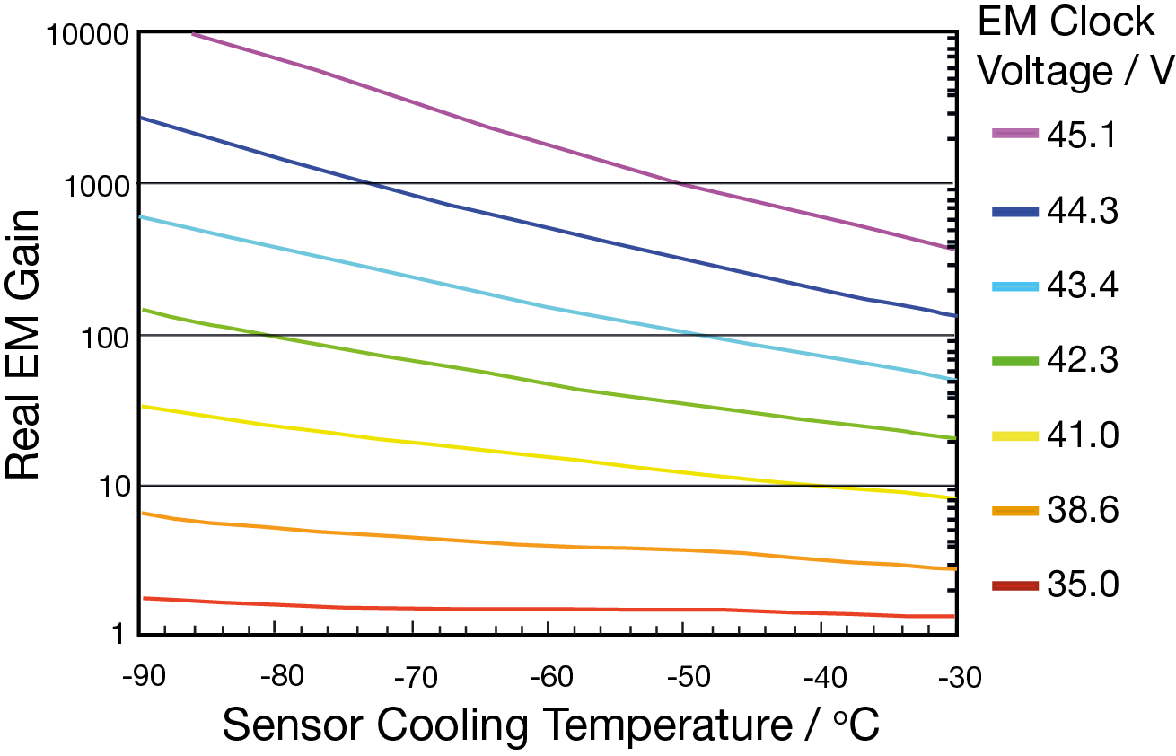
Figure 3: EM gain vs sensor cooling temperature
Aside from the EM gain ability, EMCCD cameras basically come in the same varieties as regular CCDs so they share the same properties, and Quantum Efficiencies. They also share the same noise issues of CCDs with one additional complication. The amplification process adds an additional noise which must be taken into consideration and results in a Noise Factor greater than 1. The details of this noise is covered in a later section.
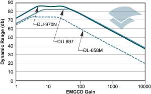
Figure 4: Dynamic range against EMCCD gain
The EMCCD gain can also complicate the dynamic range of the camera, as shown in Figure 4. Initially as the EM Gain is applied the dynamic range increases. The EM Gain reduces the effective read noise but the higher well capacity in the EM Gain register can accommodate the amplified signal. When the EM Gain register can no longer accommodate the amplified full well capacity of a pixel the dynamic range flattens. When the gain is sufficient to reduce the noise below single photon levels the dynamic range then falls off.
The exact gain a charge entering the gain register of an EMCCD sensor is impossible to know as the processes which give rise to the gain are stochastic. We can however calculate the probability distribution of output charges for a given input charge. In Figure 5 below, the probability of obtaining a distinct output charge for various input charges is plotted for a typical EM register set to a gain of 500.
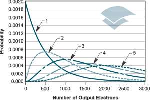
Figure 5: Probablity vs number of output electrons
If we measure an output signal of 1,000 electrons, you can see from the diagram opposite that there is a reasonable probability that this signal could have resulted from either an input signal of 1, 2, 3, 4 or even 5 electrons. At high gains (>30) this uncertainty introduces an additional noise component which is dependent on the input signal and hence acts like a Noise Factor of the EM amplifier. The details of how the Noise Factor affects the signal to noise are described in the article: Comparing EMCCD, ICCD and CCD Cameras.
In the event of when there is less than 1 electron falling on a pixel in a single exposure the EMCCD can be used in Photon counting mode. In this mode, a threshold is set above the ordinary amplifier readout and all events are counted as single photons. In this mode using a suitable high gain, a high fraction of the incident photons (>90%) can be counted without being affected by the Noise factor effect.
Because of the unique ability to boost even low signal levels so that read noise is effectively eliminated, EMCCD cameras provide a level of sensitivity that remains out of reach of the new generations of back-illuminated CMOS cameras and are therefore, an effective solution for applications in both life and physical sciences research. For example, as ultrasensitive detectors in single molecule biophysics experiments and entangled photon studies.
Take a closer look at Andor's EMCCD Cameras below...
Date: June 2021
Author: Dr Colin Coates and Dr Alan Mullan
Category: Application Note
