Resources
 Part of the Oxford Instruments Group
Expand
Collapse
 Part of the Oxford Instruments Group
Under standard operation the iXon Ultra uses the USB interface for all control and data transfer with the PC. However, some users require a more direct access to the image data stream, in order that they can perform real-time analysis, possibility using external hardware.
Such operation can be particularly important for rapid closed feedback applications such as adaptive optics. Direct real time access to data can also be useful for data intensive applications such as super-resolution microscopy or whole genome sequencing, whereby it can be desirable to carry out real time processing of data on an external GPU for example. In order to facilitate such functionality, the iXon Ultra also includes a Camera Link output.

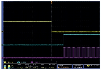
Figure 1: Latency – Vertical shift rate = 0.5μs, Time from falling edge of FIRE to rising edge of Camera Link FRAME = 494.4μs (268μs of this time is the time required to shift the image into the mask area of the sensor). Ch1: Camera FIRE (Yellow) Ch2: CL FVAL (Blue) Ch3: CL LVAL(Pink)
The Camera Link output conforms to the specification as defined by the Automated Imaging Association (AIA). Note that the Camera Link on the iXon Ultra is an output only – i.e. the serial communication interface used for camera control has NOT been implemented. When the Camera Link output is in use all camera control is still transmitted via the USB interface. The image data stream is still transmitted over the USB interface which allows other more basic analysis to be run on the PC to monitor other characteristics such as the signal level or visual feedback.
The Camera Link output is a base configuration (1-tap interface) running at 40 MHz. All data over the Camera Link interface is 16-bit greyscale. The exact pixel data type is Little Endian 16-bit unsigned integer. The Camera Link channel intercepts the image data stream in the camera head immediately after the on-head FPGA processing step, but before the USB frame buffer, therefore undergoes the same amount of on-head image processing. The data stream only contains pixel data for those pixels within the camera user defined region of interest (ROI) and hence the length of LVAL and FVAL (Camera Link ‘LINE’ and ‘FRAME’, respectively) will be dependent on the ROI defined. The user could set the camera to always transmit the same ROI and then use their Camera Link frame grabber card to extract a different ROI but they will not see any speed increase normally associated with smaller ROIs.

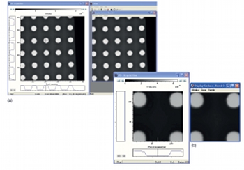
Figure 2 - Images captured using Solis (left) via USB and simultaneously in CiView (right) via Camera Link interfaces. (a) Full resolution (b) 128 x 128 ROI
The Camera Link channel intercepts the image data stream in the camera head immediately after the on-head FPGA processing step, but before the USB frame buffer, hence minimizing any latency or jitter. Figure 1 is an oscilloscope trace showing the camera ‘FIRE’ output (which goes high during the exposure), the Camera Link ‘FRAME’ (FVAL) and the Camera Link ‘LINE’ (LVAL). As you can see from the figure the delay between the exposure completing and the data appearing on the Camera Link output is ~500 μs, and most of this time is accounted for by the time it takes to move the image from the “image area” to the “storage area” on the frame transfer sensor (268 μs).
The Camera Link output has been tested using the Neon Camera Link card from Bitflow. Figure 2 show screen captures from Solis and CiView (from Bitflow), with full resolution and a 128x128 subregion. It is clear that the USB 2.0 and Camera Link interface each show identical images.
Note that when disabling the Camera Link output, the transmitter device is placed into a Powerdown Mode which tri-states the outputs. Tri-stating these outputs, along with subsequently re-enabling them, may be mistaken as valid data by frame grabber cards. Therefore, once enabled, Camera Link output should not be disabled at any time when the frame grabber card is expecting valid data.
The iXon Ultra Camera Link output should be compatible with any Camera Link interface card, but only Bitflow has been tested in house.
