Resources
 Part of the Oxford Instruments Group
Expand
Collapse
Part of the Oxford Instruments Group
Application Notes
Author: Ioannis Apergis (Uni. of Warwick), Daniel Bayliss (Uni. of Warwick), Leonidas Asimakoulas (OI Andor)
Published: 01 Dec 2025 · Last updated: 10 Dec 2025
Based on Apergis et al. 2025, RASTI, 4, rzaf049
Complementary Metal–Oxide Semiconductor (CMOS) image sensors have been developed in parallel with Charge-Coupled Devices (CCDs) for decades, but their technological trajectories diverged. While CCDs became the standard for scientific imaging, CMOS sensors rapidly advanced through commercial demand, benefitting from innovations that pushed pixel architectures to sub-micron scales [1-3]. These developments have led to CMOS devices with fast readout, low power consumption, and increasingly sophisticated performance characteristics. Recent laboratory and on-sky results now indicate that modern CMOS systems can, under the right conditions, approach or even match CCD-level performance for certain astronomical applications [4-8].
The purpose of this study is to assess whether a contemporary scientific CMOS detector can deliver the photometric stability and precision required for high quality time series astronomy. To address this, we characterise and test the Marana 4.2BV-11 sCMOS camera, under controlled laboratory conditions. The Marana combines low read noise, high sensitivity, a linear response, and a wide dynamic range, qualities that make it a strong candidate for high-precision photometry. The Marana camera offers significantly faster readout and lower effective noise than many traditional CCD cameras.
Our evaluation follows established procedures for detector characterisation, drawing in particular on the European Machine Vision Association (EMVA) 1288 standard (Version 4.0), as described in [9]. We extend this framework where appropriate to address the needs of precision photometry, allowing us to quantify the detector performance and assess its suitability for demanding time series applications.
The uses a thinned, backside-illuminated GSENSE400BSI sensor from GPixel. This 4.2 megapixel device features 11 µm pixels, a 32 mm diagonal, and employs a dual amplifier architecture. The backside illuminated, thinned structure provides high quantum efficiency across the visible range. For our setup, we selected the VIS–NIR Enhanced Unwedged window, which delivers high transmission from the optical to the red wavelengths. The sensor is housed in a sealed vacuum enclosure, enabling deep cooling and protecting against condensation. Its thermoelectric cooling system maintains temperatures down to -25°C at ambient 30°C, and with water cooling the sensor can reach -45°C under the same ambient conditions.
The Marana CMOS sensor is built around a field effect transistor architecture that enables in-pixel amplification and charge transfer. Each exposure transfers accumulated charge to a sense node, where it is amplified before readout. The detector uses a 4-transistor (4-T) pinned photodiode design [10-12], supplemented by an additional transistor that switches the pixel between High Gain (HG) and Low Gain (LG) modes. In HG mode, the sense node has a small capacitance, producing high gain and low read noise; in LG mode, the larger capacitance provides increased full well capacity at the expense of higher read noise.
During readout, each pixel’s HG or LG output is routed through corresponding column amplifiers located at the top and bottom of the sensor [13]. Low light signals are processed via the HG channel to minimise noise [14], while brighter signals are processed via the LG channel to avoid saturation [11]. These two amplification paths are combined to form the final image and are used in different configurations depending on the selected imaging mode, described in the next section.
The Marana camera offers two distinct imaging modes: the High Dynamic Range (HDR) and the Fastest Frame Rate (FFR). The HDR mode employs the HG and LG pixel-level pre-amplifiers, to capture an extended dynamic range for the image. Each pixel produces two signals (HG and LG), which are passed to the HG and LG column amplifiers, respectively, and digitised by a dual 12-bit column ADC [15-17]. A selection algorithm is implemented within the camera’s Field-Programmable Gate Array (FPGA) to identify the most appropriate channel output for each recorded pixel value, based on the saturation level of the HG channel. The LG pixel values are then scaled to match the gain of the HG channel, and the frame is being reconstructed based on the previous selection algorithm resulting in a 16-bit HDR image [11]. The HDR mode operates at 100 MHz pixel readout rate, resulting in 24 full frames per second (fps).
In FFR mode, the LG column amplifier is reassigned to operate at HG gain, giving two HG column amplifiers. Odd and even rows are read simultaneously, doubling the readout speed. The sensor outputs pixels at 200 MHz, achieving 48 fps. Since both channels are digitised with 12-bit ADCs, the dynamic range is lower than in HDR mode.
CMOS cameras exhibit amplifier glow, which may be caused by photons that are emitted by the electronics situated in the periphery of the sensor or from the excess of infrared photons emitted from the Source Follower amplifier [18].
The Marana camera comprises an on-board algorithm to subtract a pre-computed map of the glow from the image. This map is constructed by acquiring a long exposure dark image in order to capture the glow structure. The dark signal is subtracted from this image leaving behind only the signal from the glow contribution. This reference map is then scaled according to the user requested exposure time and subtracted on a pixel-per-pixel basis. This is known as an Anti-Glow correction. In our testing, we use the Marana camera with and without the Anti-Glow correction.
The Photon Transfer Curve (PTC), introduced by [18], is a standard method to characterise camera performance, providing key parameters such as the conversion gain (electrons per ADU) and Full Well Capacity (FWC). To generate the PTC, we recorded pairs of consecutive frames at increasing exposure times under constant illumination, allowing us to isolate temporal (shot) noise from spatial (fixed pattern) noise [19]. Bias frames were used to correct for Dark Signal Non-Uniformity (DSNU), and dark current was negligible due to short exposure times.
From the PTC, linear regression in the 0–70 % saturation range yields the gain: 0.632 ± 0.009 e−/ADU for FFR and 1.131 ± 0.008 e−/ADU for HDR. Using these gains the FWC was measured as 2351 e− (FFR) and 69026 e− (HDR).
The HDR mode exhibits a clear transition near 1800 ADU (right and zoomed panels of Figure 1), marking the switch from the HG to the LG channel under uniform illumination [see above; 15,16]. Because the LG channel has a higher read noise, this transition appears as a discontinuity in the PTC. Once the HG channel reaches its capacity, excess charge is read by the LG channel. Although adjusting the HG-LG gain ratio could reduce this gap, doing so would either increase read noise (lower HG gain) or reduce the LG full-well capacity (higher LG gain). For this reason, linear regression was performed only on low-signal data (0–70 % of the HG range), well below the transition region. Pixels near the HG-LG transition point can be read through either channel, depending on shot-noise fluctuations. As a result, a pixel may switch channels between frames even under identical illumination, causing abrupt changes in its output. This behaviour introduces extra variance when subtracting consecutive frames, seen as a spike in the zoomed region of Figure 1.
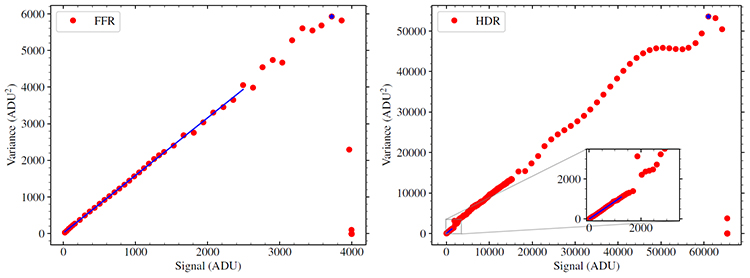
Figure 1 - Photon transfer curves for the Marana camera at -25°C. Left: The FFR readout mode. Right: The HDR readout mode. The solid blue line is a best fit linear model. The data point with the highest variance is marked with a blue star and indicates the FWC value. A zoom-in panel illustrates the transition region.
Bias is an arbitrary voltage offset added to each pixel to prevent negative values during readout, which can arise from random fluctuations in pixel signal. To characterise the bias level of the Marana camera, we performed tests in complete darkness with the camera capped to ensure no light reached the detector.
The Dark Signal Non-Uniformity (DSNU) describes the spatial noise pattern across the sensor and arises from variations in the column-level amplifiers and pixel-level fabrication defects [19]. Following the EMVA-1288 standard, we treat DSNU as the fixed-pattern noise in bias images only, isolating it from dark-current–related structure such as glow that appears in longer exposures. Since DSNU is removed in standard image reduction, it does not impact the final science frames.
We define the temporal variation of each pixel across a stack of bias images as the readout noise. This noise includes all signal-independent contributions. To isolate temporal noise from spatial structure, we analysed each pixel individually using a stack of 100 minimum-exposure bias frames arranged in a 3-D array: pixel coordinates and frame index. For all 4,194,304 pixels (2048×2048), we computed the mean and standard deviation.
The resulting distributions are shown in Figure 2. In FFR mode, the mean, median, and RMS read noise are 1.71 e-, 1.577 e-, and 1.763 e−, respectively. In HDR mode, these values are 1.697 e-, 1.571 e-, and 1.785 e−, matching Andor’s specifications. Both modes show nearly identical performance because they use the HG channel at low illumination.
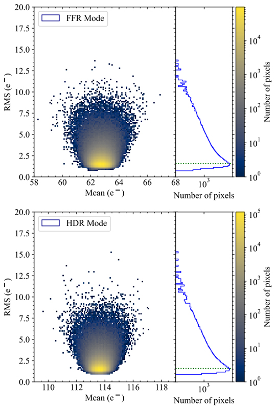
Figure 2 - Read noise distribution measured from 100 consecutive bias frames. The 2-D histogram shows the temporal noise for each pixel, while the scatter plot presents their mean values of those frames; the colour bar indicates the number of pixels. The logarithmic read noise distributions are shown in the blue histograms, with the median marked by a green dotted line. Top: Read noise distribution for the FFR mode. Bottom: Read noise distribution for the HDR mode.
In both modes, the read noise distribution is distinctly non-Gaussian with a long tail toward higher noise values. Two effects drive this: (1) pixel-to-pixel variations in the CMOS amplifier and column ADC chain, and (2) Random Telegraph Signal (RTS) noise, which pushes affected pixels to unusually large temporal fluctuations, skewing the histogram.
To measure the DSNU, we employ a set of 100 bias images. As per the EMVA-1288 standard, for modern CMOS sensors, pixels, rows and columns non-uniformities should also be included in the non-uniformity analysis. To suppress the temporal noise (i.e. read noise) we average these frames. Using the mean value of the averaged frame, the spatial variance of the image is calculated. All DSNU values are reported in electrons, having been converted from ADU using the gain. Additionally, the averaged frame is normalized by subtracting its mean to aid visualization. The distributions of the normalized averaged frames for both HDR and FFR modes are shown in Figure 3. The total, pixel, row and column DSNU was found to be 0.232 e−, 0.219 e−, 0.054 e− and 0.052 e− for the HDR mode and 0.318 e−, 0.251 e−, 0.192 e− and 0.038 e− for the FFR mode.
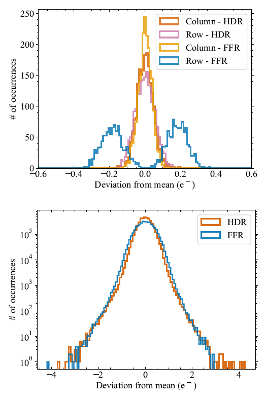
Figure 3 - Histogram distribution of the mean-subtracted pixel values used to estimate the DSNU for both readout modes. Top: Distribution of the row- and column-averaged pixel values after subtracting the spatial mean level. Bottom: Distribution of the image-averaged pixel values after subtracting the spatial mean level
Overall, the DSNU exhibits minimal variation, though it is more pronounced for the FFR mode. Notably, the FFR mode reveals a bimodal distribution in the row DSNU, as shown in Figure 3, which is attributed to the odd/even amplifier pattern . In FFR mode, row and pixel DSNU are the dominant contributors to the total DSNU, while the column DSNU remains minimal. In contrast, for HDR mode, both row and column DSNU show little variation, with pixel DSNU being the main contributor to the total.
The dark current is a signal generated in the absence of light [19]. Some electrons are excited from the valence band to the conduction band due to thermal effects within the silicon in the same way as electrons are excited from incident light. Additionally, dark current is generated by electron leakage from the photodiode or defects in the semiconductor surface, between the silicon and silicon dioxide [e.g. 20, 21]. The dark current produced electrons follow the Poisson distribution and therefore lead to dark shot noise. The dark current increases linearly with exposure time and can be minimized by cooling the sensor [22, 23].
We employed tests to measure the dark current in a dark room with the cap on to prevent illumination from background light. The integration time is adjusted to vary from 1 - 10 s with step of 1 s. We did not subtract the bias level from the dark signal data. The slope of the dark signal as a function of time yields the dark current and the intercept the bias level. The same method was used at different temperatures to investigate the dependence of the dark current with temperature.
In order to achieve temperatures below -30°C we used a water cooling system. For each frame we calculate the mean frame value. We used this method for both modes. The results are shown in Figure 4 for FFR readout mode. For simplicity, we did not plot all the linear fits and only chose to show the fit for three temperatures at +15°C, -25°C and -45°C (These are the customer default temperature settings that the camera has been optimized by Andor for best imaging performance). The slopes represent the dark current and the y-axis intercept gives the bias level. It is evident that as temperature increases the slope tends to be steeper and therefore increasing the dark current.

Figure 4 - Mean dark signal as a function of exposure time over a range of temperatures (color-coded) for the Marana camera in FFR mode. The solid lines represent the slopes at three distinct temperatures at 15°C, -25°C and -45°C. The slope measures the mean dark current of the camera. The intercept indicates the mean bias level of the system. The lower panel shows the residuals from the linear fit from the three temperatures.
For the FFR mode we find that the dark current (dark signal rate) and bias level at -25°C to be 0.736 e−pix−1s−1and 98.129 ADU respectively. For the HDR mode, we find the dark current and the bias level at -25°C to be 0.672 e−pix−1s−1 and 99.957 ADU respectively. The lower panels of Figure 4 display the residuals from the linear fit. In both modes, the Marana CMOS camera shows a considerably higher dark current compared to CCDs.
To investigate the dependence of dark current on camera temperature we used the above analysis for temperature ranging from +15°C to -55°C in steps of 5°C. The slope for each dark signal measurement with the exposures was extracted and plotted in a logarithmic scale Figure 5. The predicted dark current follows the Arrhenius behaviour [24] which is in the form of a simple exponential component.
![The logarithmic dark current as a function of the inverse temperature, following the form of [24].](https://www.oxinst.com/learning/uploads/inline-images/figure-5-20251210162347.jpg)
Figure 5 - The logarithmic dark current as a function of the inverse temperature, following the form of [24]. Top: An example dark current image showing the regions of the used for the measurements. Bottom: The dark current as a function of temperature for each region. The solid coloured lines represent the best-fit model, which is composed of the sum of two exponential functions (shown as the dotted line and the dashed line). The gray dash-dot line and squares represent the dark current of iKon-L SO Blue Sensitive CCD camera from Andor, as reported in the specification sheet.
For each region the logarithmic dark current differs, with a tendency of larger values in the glow regions, as shown in the first three plots in Figure 5. Our data are best described by a two-exponential model: at low temperatures, the dark current shows a weak temperature dependence dominated by amplifier glow, while at higher temperatures it follows a stronger thermal exponential trend. Glow-dominated regions have higher dark current values and the two-temperature behaviour is consistent across the sensor. Below 0°C, dark current is largely driven by amplifier glow, whereas above 0°C, classical thermal noise dominates.
The Photo Response Non-Uniformity (PRNU) characterizes the variability in pixel responsiveness to uniform light levels. Differences in sensor manufacturing processes can lead to variations in pixel sensitivities, causing some pixels to capture more or less electrons than others [19]. This results in a spatial structure in the frame, where each pixel exhibits a unique sensitivity profile.
To quantify the PRNU, we recorded 100 illuminated and bias subtracted images with constant light exposure at a level of approximately half the digitised saturation. We suppressed the photon shot noise components by averaging the 100 images to assess the response of individual pixels across the image [25].
A potential source of non-uniformity which is unrelated to the sensor itself is the appearance of dust or other debris on the optical window of the camera. To avoid this complication, we ensured the camera window was cleaned before testing using methanol and lens cleaning tissues. During testing, the camera was kept affixed to the light-box, to prevent any new dust accumulating on the camera window.
To evaluate the photo-response non-uniformity (PRNU), we followed the EMVA-1288 procedure, which characterises how uniformly the pixels respond when the sensor is illuminated with a flat, stable light source. We acquired 100 images at half-saturation, averaged them to suppress temporal noise, and then compared the remaining pixel-to-pixel variations against the mean signal level. A correction was applied to remove any residual temporal noise, ensuring that only spatial variations in pixel sensitivity contributed to the PRNU measurement.
Figure 6 - Histogram distributions of the photo response non-uniformities for both modes. The red bins indicate the FFR while the blue the HDR mode.
The resulting PRNU distributions for both operating modes are shown in Figure 6. The HDR mode displays a broader spread in the histogram because its half-saturation level is much higher (30,000 ADU) compared to FFR (2,000 ADU). With such a high signal level, a set of 100 images is not sufficient to fully suppress temporal noise in HDR mode, and this remaining noise contributes to the width of the distribution. In the FFR mode, the lower half-saturation level means that the same temporal-averaging strategy is more effective, resulting in a narrower distribution.
Despite these differences, the overall PRNU values are low in both modes, indicating that the camera’s pixel-to-pixel response is highly uniform. We measure PRNU values of 0.131 % in HDR mode and 0.294 % in FFR mode. Because HDR mode uses the low-gain (LG) channel at half-saturation, these results show that the LG channel is intrinsically more uniform than the HG channel used in FFR.
Linearity defines the relationship between the measured signal and the illumination level or integration time [19]. It is characterised by a linear correlation between the signal and exposure time. When treating the camera as a black box-where incident photons enter and a digitised signal is the output, linearity can be evaluated by either keeping the integration time constant while varying the light source intensity or maintaining a fixed light source while adjusting the integration time.
Measuring linearity in CMOS image sensors, particularly when employing a dual amplifier structure from the HG and LG channels, is crucial due to the presence of various effects that can impact overall linearity. In CMOS sensors with active pixel architecture, additional complications arise during the multiple process stages of the signal processing chain. This includes the linearity of the voltage amplification by the source follower transistor, as well as the linearity of the Analog-to-Digital conversion into ADU [26].
We explored how the signal changes relative to exposure time. We used a stable light source fixed while varying the exposure. For this investigation we utilised the same dataset as used in the PTC (see Section 3.1). The linearity of the camera describes how consistently the recorded signal increases with exposure time when illuminated by a stable light source. To measure this, we followed the EMVA-1288 standard, which involves comparing the measured signal at different exposure times against an ideal straight-line response. Any departure from this straight line is treated as non-linearity.
Using this method, the Marana shows excellent linearity in both operating modes. Within the standard evaluation range of 5–95% of the sensor’s full scale, the deviations from a perfectly linear response are extremely small: 0.066% in FFR mode and 0.102% in HDR mode. These results closely match the manufacturer’s specification of better than 99.7% linearity. The linearity curves for both modes are shown in Figure 7. However, the evaluation excludes the lowest signal levels below 5% of saturation. In HDR mode, the transition between the HG and LG channels occurs in this region, so it is normally not part of the linearity assessment. To explore behaviour at very low flux levels relevant to faint stars, we repeated the analysis over a broader range from 0.01-95% of full scale. Even across this much wider range, the camera remains highly linear, with deviations below 1%, although the transition region between the gain channels shows the expected small increase in residuals.
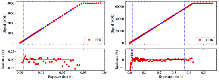
Figure 7 - Linearity measurements for the Marana in FFR mode (left) and HDR mode (right). The best fit linear model between 5% and 95% of saturation is plotted with a blue solid line. Residuals to the linear model are shown in the bottom panels. The dashed horizontal blue lines indicate the 5% to 95% boundaries we set to measure fit the linearity.
Overall, the Marana exhibits excellent linearity across both operating modes and across a wide range of signal strengths, confirming its suitability for high-precision photometry.
In this work, we set out the methodology and results for our QE testing of the Marana CMOS camera, following the approach of [8]. A halogen bulb is used in order to provide constant illumination across the visible spectrum. The light received by the photodiode is converted to electric current and measured with the use of a Keithley picoammeter. To make a measurement at a desired wavelength, Andor’s Shamrock SR-303i spectrograph is used as a monochromator. The data acquisition from both the photodiode and camera has been automated using a custom-made code. This code establishes communication with the spectrograph in order to set the slits widths, filters, and grating angle and also allows data to be retrieved from the picoammeter through an RS232 protocol.
QE measurements were performed from 400 to 1020 nm in 5 nm steps. The entrance and exit slits were set to 1000 μm, wide enough to supply adequate flux yet narrow enough to maintain a small wavelength bandpass. With this slit width, camera exposures remained short (0.001–0.01 s) to avoid saturation. A set of wavelength-appropriate filters was used to suppress stray light. For each wavelength, the photodiode current was first recorded at the monochromator’s exit slit, after which the photodiode was replaced with the Marana camera-operated in HDR mode with a fixed 0.001 s exposure and the measurement repeated.
We measure the photodiode current across a wide range of wavelengths. The responsivity curve of the photodiode is extracted from the datasheet and converted to QE values. We measure the camera flux by averaging 10 images of the same exposure after subtracting the bias level in the HDR mode. The QE was measured at 3 different temperatures; +25°C, +15°C and -45°C as shown in Figure 8. The measured QE is in close agreement with the manufacturer’s specifications within the 450–900 nm wavelength range.
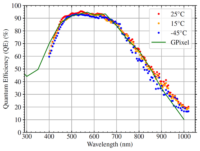
Figure 8 - QE results for Marana sCMOS camera at three temperatures. With red circles the QE at +25°C, with orange squares the QE at +15°C and with blue pentagons the QE at -45°C. The solid green line represents the QE measured by GPixel.
The Marana camera exhibits low read noise in both HDR and FFR modes. The FFR mode has comparable read noise but lower dynamic range, making it better suited for fast, high-cadence photometry of faint stars, while HDR is preferable for bright targets. Pixel-to-pixel amplifier variations and random telegraph signal noise can impact faint star detection, so correction maps or spurious noise filters are recommended. Dark current is higher than in typical CCDs and combined with glow near the edges, creating non-uniformities. To avoid photometric errors, targets should be placed away from edges, limiting the field of view and number of comparison stars. Dual-channel amplification in HDR can affect faint stars near the transition level. Overall, the Marana camera offers advantages over CCDs such as fast readout, low read noise, and no mechanical shutter, making it ideal for high-cadence time-series photometry.

© Oxford Instruments 2026
