Resources
 Part of the Oxford Instruments Group
Expand
Collapse
Part of the Oxford Instruments Group
Technical Article
Author: Oxford Instruments
Published: 01 Jan 2026 · Last updated: 14 Jan 2026
Tags: wavefront-sensors-app, UV/VIS reflectivity, UV/VIS absorption, swir-thermography, swir-laser-beam, swir-hyperspectral, swir-chemistry, swir-cameras-ps, swir-advanced-materials, swir-advanced, swir-adaptive-optics, quantum-entanglement-app, quantum transport measurements, Quantum initial phenomena, Quantum Information Processing, Quantum Hall Effect, Quantum dots , Quantum dot measurements, Quantum computing, Plasma, Large area deposition, large area, ixon-emccd-ps-lr, istar-training-school-webinars, istar-training-school-piv-mode, istar-training-school-internal-trigger, istar-training-school-external, istar-training-school-beginner, istar-training-school-advanced, ikon-ccd-long-exposure, ikon-ccd-learning, Astro Cameras Page
Accumulation is the process by which data acquired from a number of similar scans are added together in computer memory.
Acid etching is a technique that uniformly thins CCDs to approximately 10 µm so that an image can be focused on the back of the parallel register (where there is no gate structure).
An Acquisition is taken to be the complete data capture process.
An adapter is a device that allows a CCD camera to be attached to a variety of scientific instruments or lenses. It is also referred to as a mount adapter and lens mount adapter.
Analog is a scheme for representing data via continuous amplitudes.
An analog-to-digital converter is the electronic circuitry in a CCD camera system that converts the analog information (continuous amplitudes) acquired by the detector into digital data (quantified, discrete steps) used for image display.
An ADU is a number representing a CCD’s output. The relationship between ADUs and the number of electrons acquired on the CCD is defined by the system gain. Intensities given in ADUs provide a convenient method for comparing images and data generated by different cameras.
An angstrom is a unit of measure equal to 0.1 nanometers.
An arc lamp is often used as a light source on a microscope. It is an electric light in which a current traverses a gas between two incandescent electrodes and generates an arc that produces light. Arc lamps have a limited lifetime.
Background is a data acquisition made in darkness. It is made up of fixed pattern noise, and any signal due to dark current.
A back-illuminated (back-thinned) CCD is a CCD that has been uniformly reduced to a thickness of approximately 10 µm so that an image can be focused on the back of the parallel register (where there is no gate structure). Thinned CCDs exhibit high sensitivity to photons ranging from the soft X-ray to the near-infrared regions of the spectrum. Since light hits the silicon directly instead of passing through the gate structure, sensitivity to blue light is particularly good. Many back-illuminated CCDs also have ultraviolet coatings that “down convert” UV light into the visible portion of the spectrum, further increasing QE.
Binned readout is, within a CCD, the process of moving charge that has been binned to an output amplifier for conversion to an image.
Binning is a process that allows charge from two or more pixels to be combined on the CCD-chip prior to readout. Summing charge on the CCD and doing a single readout results in better noise performance than reading out several pixels and then summing them in computer memory, because each act of reading out contributes noise. The two main variants are vertical binning and horizontal binning, and there are several binning patterns that tailor these variants to typical application usage.
Vertical binning is one of the two main variants of binning, involving combination of charge in the vertical (parallel) direction on the CCD prior to readout.
Horizontal binning is one of the two main variants of binning, involving combination of charge in the horizontal (serial) direction on the CCD prior to readout.
A binning factor is the number of pixels to be combined on a CCD during binning. A binning factor of 2×2 means pixels in two rows and two columns (four pixels total) are combined for CCD readout.
Bit depth is the number of bits (smallest unit of information in the binary system) that are digitized by a system’s A/D converter.
A BNC connector is a connector used to couple coaxial cables to high-frequency electronic equipment, such as a video monitor.
Bulb mode is a type of exposure in which a trigger signal from an external source controls both the start and end of the exposure.
In CCD imaging technology, charge is a measure of the number of electrons confined by a pixel.
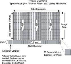
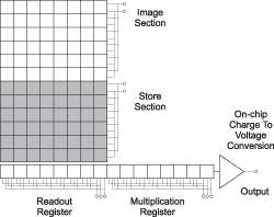
A charge-coupled device is a silicon-based semiconductor chip bearing a two-dimensional matrix of photo-sensors, or pixels, referred to as the image area. Pixels can be considered arranged in rows and columns. A typical CCD chip may comprise 256 rows and 1024 columns, or 578 rows and 385 columns. The CCD in a detector is a scientific slow scanning device, in contrast to a fast scan CCD used in video cameras to capture moving images.
A typical CCD layout includes light-collecting rows (image area) and a shift register that runs below and parallel to those rows. The shift register has the same number of pixels as a light-collecting row but is masked so no light falls on it. When light falls on an element, photoelectrons are produced and confined to their respective elements. Thus, if an image pattern is projected onto the array, a corresponding charge pattern is produced. To capture this pattern into computer memory, the charge pattern must be transferred off the chip. Transparent electrodes covering the array are clocked to shift the entire charge pattern one row at a time down into the shift register. The shift register has electrodes (vertical, parallel to columns) that transfer charge packets one element at a time into the output node of the on-chip amplifier. The amplifier output feeds the A/D converter, which converts each charge packet into a 16-bit binary number.
Charge smearing refers to the ability of a CCD to transfer charge in each pixel to the next without loss during transfer, described via charge-transfer efficiency (CTE). Scientific-grade CCDs typically have CTE of 99.9998%, where 100% is perfect. The term can also refer to the process by which electrons in one potential well are moved to an adjacent well.
Charge transfer can refer to residual charge left behind in potential wells when an image is shifted within a CCD.
A C-mount is a standard screw-in lens mount common to many scientific instruments. Thread: 1-inch diameter, 32 threads/inch. Back focal length: 17.52 mm.
In digital imaging, convolution is the replacement of each pixel’s gray level with a new value adjusted to take into account neighboring pixel values. Whether an image is smoothed or sharpened depends on the calculations performed.
Cooling refers to cooling the CCD using a thermoelectric (TE) cooler. TE coolers are electrically powered devices with no moving parts, acting as heat pumps that transfer heat from the CCD (cold side) to a heat sink (hot side). The minimum CCD temperature depends on heat sink temperature. A vacuum design can enable very large temperature differentials. The maximum temperature difference attainable depends on heat load created by the CCD, number of cooling stages, and operating current.
Air cooling removes heat from the heat sink using a built-in fan. It is convenient but does not achieve as low a CCD temperature as water cooling. Even with a fan, a heat sink typically must be ~10°C hotter than room air to transfer heat effectively; thus minimum CCD temperature depends on room temperature.
Water cooling circulates external water through the heat sink using connectors on the camera head. It removes heat efficiently, keeping the heat sink within ~1°C of water temperature; thus minimum CCD temperature depends on water temperature, not room temperature. Chilled water or a recirculator can achieve lower temperatures than air cooling.
If water temperature is lower than the room dew point, condensation will occur on the heat sink, taps, and other metal parts, which can quickly destroy the head and must never be allowed. A recirculator can eliminate the dew point problem.
A temperature sensor on the CCD combined with feedback control of cooler current allows stabilization of the CCD to any desired temperature within the cooler operating range, so operation does not simply vary with heat sink temperature.
Counts refer to the digitization by the A/D conversion and are the basic units in which data are displayed and processed. Depending on the device, one count may correspond to, for example, 10 photoelectrons in a pixel.
Correlated double-sampling readout is a sampling technique for higher precision: the sampling circuit is reset to a predetermined reference level, then the pixel voltage is sampled and the difference is computed. This correlation minimizes read noise, especially in ultra-low-noise cameras.
Cropped Sensor Mode is a specialized readout mode for achieving sub-millisecond temporal resolution from EMCCD and CCD cameras. It uses a user-defined sub-array within the full sensor area that covers the region of rapid change. The sensor “imagines” it is this smaller array via software executing special readout patterns, and reads out at a proportionally faster frame rate.
Dark current is the charge accumulated within a well in the absence of light, and also the background current that flows in a CCD or image intensifier system. Cooling the CCD photoconductor or intensifier photocathode can reduce or eliminate dark current.
Dark noise is the statistical variation of the dark current, equal to the square root of the dark current. Dark current can be subtracted from an image, while dark noise remains.
Dark signal is the charge (often expressed in electrons) produced by dark current during exposure time. All CCDs produce dark current measurable typically in tenths of milliamps per pixel. Dark signal adds to measured signal and increases noise; it varies strongly with temperature, can increase background over time, and limits useful exposure time. Reducing temperature reduces dark signal (typically, for every 7°C drop, dark signal halves). Since CCD readout noise is low, detectors should be cooled to avoid shot noise from dark signal compromising performance. For exposures less than a few seconds, cooling below 0°C generally removes most shot noise caused by dark signal.
A deep-depletion CCD is designed for enhanced near-infrared and high-energy X-ray sensitivity by applying a bias voltage to a thick layer of high-resistivity silicon to create a deeper depletion region than conventional CCDs. This allows longer-wavelength photons to interact in the layer rather than pass through.
Detection limit is the smallest signal detectable in a single readout, defined when the signal level equals the noise accompanying it (S/N = 1). Noise sources include shot noise of the signal, shot noise of any dark signal, and readout noise. If the signal is small, its shot noise can be ignored, and with low temperature and short exposure the lowest detection limit equals the readout noise.
A diffraction grating disperses light into a spectrum using closely spaced parallel grooves (often several thousand per cm) producing interference that separates components of the incoming light. It can be the main dispersing element in a spectrograph. Grating equation in the form: m(λ) = d sin(θ) (with variables described as m order number, λ wavelength, d groove spacing, θ angle of incidence.
A transmission grating has grooves ruled on transparent material (glass or Perspex). Light passing through splits into orders with spectra on either side; in each order blue is diffracted least and red most. Orders increase in dispersion and faintness with distance from the direct beam.
A reflection grating has grooves ruled onto a reflective coating on a surface that can be plane or concave (concave can focus light). An advantage is producing a spectrum from ultraviolet to infrared since light does not pass through grating material.
Digital is a scheme for representing data via quantized, discrete steps.
To digitize is to convert data (or images) into a digital format.
Dynamic range is the ratio of maximum (brightest) to minimum (darkest) signal levels present in an image. A true 12-bit camera can provide a dynamic range of 4096:1.
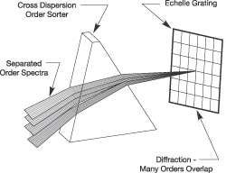
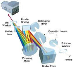
An echelle grating has widely spaced grooves with a zigzag or step-like cross-section. Light falls at right angles to the groove faces, producing overlapping spectra with high resolution. A second low-dispersion grating or prism arranged perpendicular to the echelle separates the overlapping spectra.
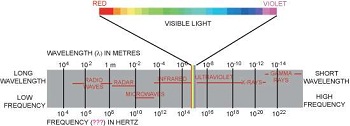
Electromagnetic waves are produced by the motion of electrically charged particles and radiate from them. They travel through empty space and through substances like air. EM radiation can be defined by wavelength, frequency, and energy. Relationships noted include Frequency = speed of light / wavelength, Energy = constant × frequency, and also E = mc².
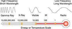
The electromagnetic spectrum describes radiation spread across many wavelengths: radio, microwaves, infrared, visible, ultraviolet, X-rays, gamma rays, and others. There is no definitive boundary between categories; portions blend. Wavelength (and dependent properties frequency and energy) is the fundamental differentiator. Different wavelengths/energies produce different effects: radio waves have long wavelength/low energy so eyes can’t detect them and they pass through bodies; antennas/electronics capture them. Infrared is readily absorbed and converted to heat. X-rays can pass through soft tissue but are stopped by bone.
An EMCCD camera uses an Electron Multiplying CCD: a silicon chip with a two-dimensional pixel matrix (image area). It is like a conventional CCD but with the shift register extended to include an additional gain register that multiplies electrons, enabling ultra-sensitive low-light detection up to single-photon detection.
Etaloning is an effect in standard back-illuminated CCDs caused by reflections between parallel front/back surfaces, creating interference fringes (constructive/destructive). It causes semi-transparency in the near-infrared.
Exposure time is the length of time a CCD accumulates charge.
A faceplate is the front surface of a camera head, often incorporating a window. It may be used to support a target or mount the camera head.
A fiberoptic-coupled CCD has a coherent fiberoptic bundle bonded to the CCD’s imaging surface to transfer an image source to the CCD.
Fiberoptics (optical fiber) is the medium and technology used to transmit information as light pulses through very fine flexible glass or plastic fibers (often ~120 µm diameter).
Fill factor relates to the light-gathering area of a CCD. A 90% fill factor means 10% of each pixel area is insensitive to light.
An F-mount is a standard lens mount common to many scientific instruments with back focal length 46.5 mm.
Fps means frames per second.
A frame is one image moved from a CCD in a full parallel shift.
A frame buffer is the hardware containing frame memory (RAM) that stores full frames of the image signal.
A frame-transfer CCD divides the parallel register into an image array (collection) and storage array (storage). After exposure, charge is shifted to storage and read out. It can operate without a shutter and run continuously at high rates.
A front-illuminated CCD is one in which the gate structure is located in front of the potential wells.
A full-frame CCD uses the entire active parallel register to expose photons and integrate/transport charge. It uses a shutter to control exposure and block light during readout to prevent smearing.
Full well capacity is the number of electrons that can be held in one potential well. It is assumed pixels have the same well size and capacity.
As gain increases, at some point dynamic range decreases. This occurs when gain equals readout noise (in electrons). At 1 MHz readout, dynamic range is maintained over 20,000:1 for gains up to ~20×, while at 62.5 kHz it is maintained over 43,000:1 for gains up to ~6×. Higher gain for sensitivity requires a trade-off with dynamic range; to preserve dynamic range, avoid using higher gain than necessary.
The gain register output feeds a conventional CCD output amplifier that has readout noise of a few electrons rms, and around 10–20 electrons rms at MHz readout rates. This noise is effectively reduced by the multiplication factor so that, when high enough, effective noise can fall below 1 electron rms. Thus gain can make amplifier noise insignificant at any readout speed. However multiplication adds noise due to statistical nature (similar to ICCD Noise Factor). With no gain, no extra multiplication noise. At high gain, additional noise can be √N (N = signal electrons), adding to shot noise to become √(2N). If signal is above read noise, gain may be unnecessary and should be reduced/off; if signal is lost in read noise, increasing gain enables detection, including single-electron events that appear as spikes several hundred counts high. In Andor EMCCD cameras, gain is limited to a maximum of 255× at −50°C for standard systems, comparable to high-end ICCDs.
In an EMCCD, a gain register is placed between the shift register and the output amplifier. Electrons are multiplied in the gain register by impact ionisation.
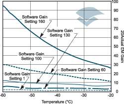
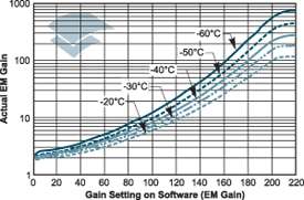
EMCCD gain varies with temperature: multiplication increases as temperature decreases. At room temperature gain is reduced. Because of this dependence, cooling is recommended so temperature (and thus gain) is stabilized. The graph below shows typical gain multiplication vs software gain settings at various temperatures.
Gate structure refers to the polysilicon structure located on the parallel register. Polysilicon gates are transparent at long wavelengths but become opaque at wavelengths shorter than 400 nm.
In an ICCD camera system, gating is the application of a voltage that switches the image intensifier on/off in very short intervals. This improves temporal resolution.
Gray level is pixel brightness expressed as an integer. Levels range 0–255 for 8-bit, and 0–4095 for 12-bit.
An HCCD camera is a high-performance CCD camera using advanced design (low-noise electronics, cooled detector) optimized for scientific or industrial imaging.
High-speed framing is the process of reading frames from a CCD at a rapid rate.
A host computer is the primary or controlling computer for a digital camera.
An ICCD camera is an intensified CCD camera: a digital imaging/spectroscopy system using an image intensifier coupled to a CCD. These cameras offer high sensitivity in ultra-low-light conditions; gating can improve temporal resolution.
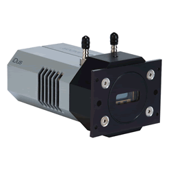
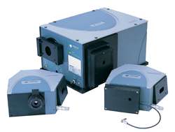
iDus is described as Andor’s USB CCD camera for spectroscopy.
An image array is the portion of a frame-transfer CCD exposed to light where the image is collected. After exposure, charge is shifted to the storage array.
Image averaging reduces random noise by averaging a pixel’s brightness across a series of successive frames.
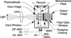
An image intensifier amplifies image intensity (brightness), not image size. It is typically 1–2 inches in diameter and about 1 inch thick. An image is projected onto the input window and an intensified image appears on the exit window (often a fiber optic plate). Intensifiers can be rapidly switched on/off, acting as a fast shutter. Tubes may be GEN II or GEN III. The system described is proximity-focused, compact, and easily gated to ~2 ns timescales. Three major elements determine performance: the photocathode, microchannel plate (MCP), and output phosphor screen.
InGaAs is a material used in some detectors (e.g., PDAs) to provide higher QE in the near-infrared.
Indium tin oxide is a material used in some CCD gates to provide higher QE, particularly in the blue-green region.
Infrared is the region beyond the visible spectrum at the red end, typically greater than 770 nm.
Integration is the act of accumulating signal or charge on a CCD.
An interline mask consists of opaque strips spanning an interline-transfer CCD that function as storage areas.
An interline-transfer CCD subdivides the parallel register so opaque strips mask columns of pixels and act as storage areas. During exposure, image accumulates in exposed photosites; the image shifts under the interline mask in the serial register for readout. Integrated charge can shift quickly (~200 ns) into storage areas.
iStar is Andor’s ICCD camera for low-light spectroscopy requiring fast gating.
iXonEM+ is Andor’s first commercially available EMCCD camera for ultra-sensitive dynamic digital imaging.
Light is a form of electromagnetic radiation. Visible light (400 nm to 770 nm) can be perceived by the unaided human eye.
Linearity means an object that is twice as bright as another will appear exactly twice as bright in the resultant image.
Liquid nitrogen cooling cools the CCD by direct contact of LN to the CCD cold block. CCDs are not run at LN temperature (−200°C) because charge-transfer efficiency begins to suffer at very low temperatures. Operation is usually regulated between −120°C and −60°C to decrease dark current without unduly compromising CTE.
LucaEM: “Luca” is shorthand for Last Universal Common Ancestor and is described as Andor’s latest mid-market EMCCD camera.
Mechelle is Andor’s spectrograph based on the echelle grating principle and patented optical design, providing extremely low cross-talk, equally spaced order separation, and maximum resolution. The Mechelle range offers simultaneously recorded wavelength range from UV to NIR with very high resolution and no overlapping wavelengths.
A megapixel is a CCD whose imaging array contains at least one million pixels.
A microchannel plate is a major component of an image intensifier: a slightly conductive glass substrate with millions of parallel channels containing secondary electron emitters on the channel walls. Each channel acts analogously to a photomultiplier.
Microlenses are small lenses that increase fill factor in interline-transfer CCDs by redirecting incident light away from masked storage columns toward photosensitive areas.
MPP (inverted operation) reduces dark current generation rate by a factor of 20 or more, relaxing cooling requirements so that thermoelectric cooling is sufficient for many applications.
Near infrared is the spectral region from about 0.77 µm to about 3.0 µm.
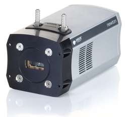
Newton is described as the world’s first spectroscopic camera with EMCCD technology. EMCCD amplifies very low light signals above the CCD read noise floor and uses solid-state electron multiplication based on impact ionisation in silicon.
Noise is described as complex and can be broken into two broad categories: pixel noise and fixed pattern noise.
An opaque mask is light-impenetrable material used to shield selected parts of a photosensitive surface. Opaque masks are used in interline-transfer CCDs and frame-transfer CCDs.
In a CCD, the origin is the point located closest to the output node.
The output amplifier amplifies electrons in the output node sufficiently to reach the A/D converter. It is the primary source of read noise.
The output node is the location (often a single pixel adjacent to the serial register) where charge is collected as a discrete picture element for CCD readout. Data enters from the serial register and exits to the A/D converter.
Parallel (vertical) binning is the accumulation of multiple rows of charge in a CCD’s serial register, defined by the user-specified binning factor.
Parallel binning factor is the number of pixels (in the parallel direction) shifted to the serial register, read out, and processed into an image, specified in software prior to exposure.
In the serial, parallel (s, p) coordinate system, the parallel direction begins at the origin and runs perpendicular to the serial register.
Parallel offset is, when defining an ROI, the distance (in pixels) between the serial axis and the rectangular/square exposure area.
The parallel register is a large square array containing many potential wells (pixels). Charge accumulates here during exposure and forms an image when shifted and read out.
Parallel shift is columnar movement of charge from one or more pixels to an adjacent row, continuing until the number of pixels to be binned are emptied into the serial register.
Parallel size is the ROI size in pixels extending in the parallel direction.
The Peltier effect is heat transfer opposite the direction of current flow. Pumping current through a Peltier stack to a heat sink removes heat from a CCD; the heat sink is cooled by circulating liquid or air and must be regulated.
A phosphor is a chemical substance that fluoresces when excited by X-rays, an electron beam, or ultraviolet radiation. Phosphors are often rare earth oxides/halides and usually emit green light with decay times from hundreds of nanoseconds to a few milliseconds.
A phosphor screen is a major component of an image intensifier. Electrons exiting the MCP are accelerated and strike the screen, converting them back into photons for CCD detection.
A photocathode is a major component of an image intensifier. Coatings convert some incident photons into electrons. High QE is critical because photons not captured are lost from the final signal.
A photodiode array is a linear array of discrete photodiodes on an integrated-circuit chip used in digital detection systems.
Photometry is measurement of light properties, particularly luminous intensity.
Photon-noise-limited operation is operating a detection system so that photon (shot) noise is the dominant noise source, implying other noise sources are low.
A pixel (picture element) is the smallest element in a visual display.
Pixel noise can be defined as the variation in values read when reading the same pixel repeatedly. RMS variation is often used; RMS is typically 4–6 times smaller than peak-to-peak variation. Pixel noise has three main constituents: readout noise, shot noise from the dark signal, and shot noise from the light signal itself. Shot noise cannot be removed and is √(signal electrons). Readout noise is due to amplifier/electronics, largely independent of signal and dark levels, slightly temperature dependent, present on every read, and sets the best achievable noise limit. Dark shot noise depends on exposure time and strongly on temperature; signal shot noise depends on signal level. If signal or dark signal is zero, its shot noise is zero. Total pixel noise is approximated by root-sum-square:
Total = sqrt(readnoise² + darkshot² + sigshot²)
Fixed pattern noise (FPN) is pixel-to-pixel differences in readout values even with no light, remaining constant from read to read. It arises partly from dark signal variations and partly from fabrication irregularities. Because it is fixed, it can be completely removed by background subtraction. It can change if temperature changes since part is due to dark signal.
On-chip multiplication gain is technology that multiplies charge collected in each pixel. Secondary electrons are generated via impact ionization initiated by higher-than-typical voltages applied to an extended portion of the serial register. Multiplying signal above output amplifier read noise enables ultra-low-light detection at high speed. Some cameras have both a multiplication-gain amplifier (low-light high-speed) and a traditional amplifier (wide dynamic range).
A Poisson distribution is a probability function used to model the density of counts of randomly occurring events obtained during a specified interval of time.
A potential well is a discrete region within the CCD imaging array where an incident photon may be trapped (i.e., a pixel).
Qualitative analysis is evaluating the appearance of an acquired image.
Quantitative analysis is measuring and comparing the intensity of light incident on individual pixels.
Quantum efficiency is the effectiveness of an imager at producing electronic charge from incident photons and is especially important for low-light imaging.
Radiometry is the science of measuring electromagnetic radiation, often using a radiometer.
Raman is a radiation effect used in spectroscopy (Raman scattering), named after Sir Chandrasekhara Venkata Raman. It is used in condensed matter physics and chemistry to study vibrational, rotational, and other low-frequency modes. It relies on inelastic scattering of monochromatic light (often from a laser in visible, near-IR, or near-UV). Phonons or other excitations are absorbed or emitted, shifting photon energy up or down. The energy shift provides information about phonon modes.
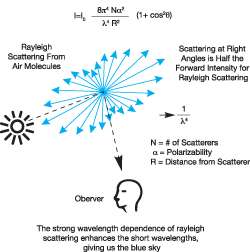
Rayleigh scattering is scattering of light from molecules in the air (and can extend to particles up to about a tenth of the wavelength). Rayleigh scattering gives the blue sky. It can be considered elastic scattering since scattered photon energies do not change. Scattering where scattered photons have higher or lower energy is Raman scattering; this often involves exciting molecular vibrations (lower energy photons) or scattering off an excited vibrational state (higher energy photons).
Read (pre-amplifier) noise is unwanted signal/disturbance generated by the on-chip output amplifier. It can be reduced to a few electrons by modifying operating conditions.
Read-noise-limited operation is when read noise exceeds photon (shot) noise. It is undesirable because image data are limited by experimental restrictions or deficiencies in camera design.
Readout is the process by which data are taken from CCD pixels and stored in computer memory. Pixels are read out individually in sequence (arranged in a single row for readout order). Readout involves amplifying charge into a voltage, performing A/D conversion, and storing data. The time taken is the “read time.”
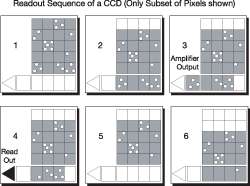
A CCD readout sequence (as described) proceeds:
Exposure to light builds a charge pattern on the image area.
Frame charge shifts vertically by one row so the bottom row moves into the shift register.
Charge in the shift register moves horizontally by one pixel so the endmost pixel charge moves into the output node.
Charge in the output node is passed to the A/D converter and read out.
Steps 3–4 repeat until shift register is emptied.
Frame shifts vertically again and the process repeats until the whole frame is read out.
This sequence corresponds to a default “Full Resolution Image” binning pattern; other patterns sum charge in shift register and/or output node prior to readout.
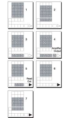
An EMCCD readout sequence proceeds:
Exposure builds charge pattern on the Image Area.
Charge shifts vertically by one row so bottom row moves into the shift register.
Shift register charge moves horizontally by one pixel so endmost charge moves into the gain register.
Charge shifts into the output node of the amplifier.
Charge in the output node passes to the A/D converter and is read out.
Steps 3–4 repeat until shift register empty, then the frame shifts vertically and repeats until the whole frame is read out. Other binning patterns sum charge in the shift register and/or output node (see binning).
Recirculation is a refrigeration process in which water is forced-air cooled then pumped around a circuit, widely used in research and test laboratories.
Region definition is the designation of a rectangular/square area on a CCD to be exposed as an image, defined by coordinates in the serial, parallel (s, p) coordinate system.
An ROI is a user-defined rectangular area (often square) on a CCD that is exposed and processed as an image.
Resolution is how fine a detail can be detected, in terms of space (spatial), time (temporal), or intensity.
Saturation is the largest signal the CCD can measure. It relates to how much charge builds up in pixels; multiple factors determine the maximum charge the CCD can handle.
Scanning is continual scanning of the CCD to prevent saturation with dark current (dark signal). In a keep-clean scan, the charge is discarded. In an acquired scan, charge undergoes A/D conversion and is acquired into memory for processing/display; i.e., it is read out.
A scientific-grade CCD is a high-performance CCD with fewer defects than commercial-grade devices. It provides better spatial resolution, lower noise, and enables accurate intensity measurements.
SDK refers to the AndorMCD Software Development Kit. It provides programmer access to Andor CCD and ICCD cameras. The key element is the 32-bit DLL “ATMCD32D.DLL,” usable with C, C++, Visual Basic, LabVIEW, and other environments.
Serial (horizontal) binning is accumulation of charge from two or more pixels of the CCD’s serial register into the output node before shifting for readout.
Serial binning factor is the number of pixels in the serial direction shifted to the output node, read out, and processed into an image, specified in software prior to exposure.
Serial direction is, in the serial, parallel coordinate system, the direction beginning from the origin and moving away parallel to the serial register.
Serial offset is, when defining an ROI, the distance (in pixels) between the parallel axis and the user-defined rectangular/square exposure area.
This is a CCD nomenclature based on the corner closest to the output node on the parallel register (origin). Coordinates increase away from the origin. s represents the serial coordinate and p the parallel coordinate.
The serial register is a row of pixels adjacent to the parallel register. It receives charge from the parallel register and shifts it to the output node to form an image.
Serial shift is the movement of charge along the serial register pixel by pixel toward the output node, where the charge is processed as an image.
Serial size is the ROI size in pixels extending in the serial direction.
Shamrock is Andor’s range of Czerny-Turner spectrographs with models Shamrock SR-303i and Shamrock SR-163/SR-163i.
The shift register is typically a single row of elements running parallel to and below the bottom row of light-gathering pixels (image area). It is protected from light by an aluminum mask. Its elements have greater charge capacity (greater well depth) than other pixels.
Shot noise is fundamental and cannot be removed. Any signal (dark or light) has shot noise. If signal (or dark signal) = N electrons, shot noise = √N. You cannot remove signal shot noise, but by minimizing exposure and lowering temperature you can reduce dark signal and its shot noise.
SNR (S/N) is the ratio between a signal and the noise associated with it. Noise has fixed components and variable components (shot noise √signal). SNR generally improves as signal increases. Maximum SNR is the ratio between maximum signal (saturation) and the noise accompanying it; near saturation, shot noise of the signal dominates.
Silicon is a tetravalent, nonmetallic element used to fabricate CCDs.
A slow-scan CCD has special circuits allowing slower-than-standard readout rates to reduce read noise.
A spectrometer is an optical instrument that allows viewing, recording, and analyzing a spectrum by making component waves distinct and visible.
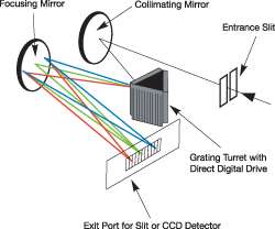
A spectrograph is an optical instrument that uses dispersed light to produce spectra. Components and functions:
Spectroscopy is the branch of science dealing with theory and interpretation of spectra. Spectra are regions of the electromagnetic spectrum.
In a frame-transfer or interline-transfer CCD, the storage array is the portion of the parallel register covered with an opaque mask for temporary charge storage.
Superpixels are the result of combining vertical binning and horizontal binning. Multiple pixels are binned and read out as one large pixel, effectively forming a matrix of superpixels.
Subarray readout is moving charge from a user-defined rectangular/square subregion to an output amplifier for conversion to an image.
System noise is unwanted signal in an image caused by internal interference and other factors. Many noise sources exist, but three account for the majority: dark noise, photon (shot) noise, and read noise.
Temporal resolution is defined as the frequency at which images are recorded/captured at a specific place. More frequent capture means better temporal resolution.
TDI is an integration and CCD readout mode that allows acquisition of long swaths of a moving image.
Thermoelectric cooling is pulling heat away from a CCD using Peltier cooling devices.
Thinning is the process (often via acid etching) of uniformly reducing CCD thickness to approximately 10 µm so an image can be focused on the back of the parallel register where there is no gate structure.
A trigger is a signal (typically TTL) transmitted to synchronize two or more instruments, acting like an initiator in a process.
USB stands for Universal Serial Bus, a standard computer interconnection system introduced in 1995 by Intel, Compaq, Microsoft, and other companies.
Ultraviolet is the region of the spectrum from about 400 nm (just beyond visible violet) to about 40 angstroms (on the border of the X-ray region).
X-rays are electromagnetic radiation with wavelengths in the range 10 nm to 100 pm (frequencies ~30 PHz to 60 EHz). They were discovered in 1895 by Wilhelm Conrad Röntgen and are sometimes called Röntgenstrahlen in German-speaking countries. Oxford Instruments Andor manufactures CCD detection systems for a range of X-ray applications.

© Oxford Instruments 2026
