Resources
 Part of the Oxford Instruments Group
Expand
Collapse
Part of the Oxford Instruments Group
Application Notes
Author: M. M. Sonner, H. J. Krenner
Published: 01 Feb 2019 · Last updated: 25 Sep 2023
III-V semiconductor nanowires (NW) can be regarded as very promising candidates for future high-performance nanoelectronic and nanophotonic devices [1]. NWs enable the integration of the superior electronic and optical properties of direct bandgap III-V semiconductors onto the well-established silicon platform. This is due to the effective strain relaxation mechanism at the silicon/nanowire interface.
Here, we report on the effect of the crystal structure on the optical properties of GaAs-AlGaAs core-shell nanowires.
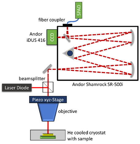 Figure 1: Schematic of the experimental setup.
For single nanowire photoluminescence (PL) spectroscopy, a homebuilt micro-photoluminescence setup is used as illustrated in Figure 1. For the measurements, NWs were first transferred onto the substrates from solution via drop-casting. Further on, the samples were mounted in a liquid helium flow cryostat which is cooled down to temperatures below 10K. Well-isolated individual NWs are excited by a picosecond pulsed laser diode at a wavelength of 660 nm while the laser is focused to a spot size of around 2 μm2 by a 50x objective. The objective is mounted at a high-precision closed-loop piezo-system (scan range: 80 µm x 80 µm) allowing us to record high-resolution intensity profiles over a large area by scanning the laser spot. The PL emission of the NWs is dispersed by an Andor Shamrock SR-500i-D1-SIL spectrograph. The spectrograph is equipped with a thermo-electrically cooled CCD detector (Andor iDus DU416A-LDC-DD) for quick multichannel acquisition. The grating turret of the spectrograph is equipped with 300 lines/mm (blaze 760 nm), 600 lines/mm (blaze 800 nm) and 1200 lines/mm (blaze 750 nm). These gratings are silver coated to ensure for optimum performance in the target wavelength range. For PL-lifetime measurements, the second (side) output port of the spectrometer is equipped with a X-Y fiber coupler (with Slit Assembly) which allows us to couple light into a multi-mode optical fibre guiding the signal towards a single photon avalanche diode (SPAD).
Figure 2 shows a typical PL intensity mapping of a GaAs-AlGaAs core-shell NW at low temperatures of about 10 K. In this experiment, the laser is scanned across the sample and a spectrum is recorded at each position. In Figure 2a the integrated intensity map of the NW is shown. The NW is clearly visible with a maximum intensity at one end of the NW. In Figure 2b and Figure 3a, a low-temperature PL spectral map and single PL spectrum of the NW recorded at the centre of the NW are shown, revealing a double peak structure.
The two peaks separated by about ΔE=26 meV. Here, Peak 1 at 1.488 eV is attributed to emission from localized excitons at a single twin plane defect [2,3]. Twin defects commonly occur in these NWs due to the inclusion of wurtzite crystal phase segments within the otherwise zincblende crystal structure. This leads to the formation of so-called indirect excitons with holes confined in the twin wurtzite segment and electrons in the surrounding zincblende structure [2,3,4]. In order to identify the origin of the two emission peaks we performed time-resolved PL. At 1.514 eV, the time transient exhibits a clear mono-exponential decay with a characteristic lifetime of τ ∼ 0.7 ns, which is consistent with literature values for free excitons in GaAs nanowires. In contrast to the mono-exponential decay of emission peak 2, multi-exponential decay is observed at 1.488 eV. In addition to the fast decay, an increased exciton lifetime is characteristic for the spatial separation of electron free exciton.
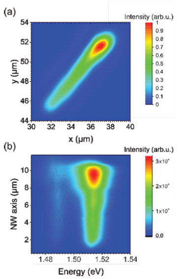
Figure 2: (a) Intensity mapping of a GaAs-AIGaAs core-shell nanowire. (b) Map of the PL spectrum recorded along the NW axis at 10 K.
The Shamrock 500i spectrograph equipped with the Andor iDus 416 CCD camera and the X-Y Fiber Couplers enable us to examine the optical properties of semiconductor nanowires.
[1] J. Appenzeller, J. Knoch, M. T. Björk, H. Riel, H. Schmid, and W. Riess, “Toward nanowire electronics”, IEEE Transactions on Electron Devices 55(11) (2008), 2827–2845.
[2] M. Heiss, S. Conesa-Boj, J. Ren, H. Tseng, Ad. Gali, A. Rudolph, E. Uccelli, F. Peiró, J. R. Morante, D. Schuh, E. Reiger, E. Kaxiras, J. Arbiol, and A. Fontcuberta i Morral, “Direct correlation of crystal structure and optical properties in wurtzite/zincblende GaAs nanowire heterostructures”, Phys. Rev. B 83 (2011) 045303.
[3] D. Rudolph, L. Schweickert, S. Morkötter, L. Hanschke, S. Hertenberger, M. Bichler, G. Koblmüller, G. Abstreiter, and J. J. Finley, “Probing the trapping and thermal activation dynamics of excitons at single twin defects in GaAs–AlGaAs core–shell nanowires”, New Journal of Physics 15 (2013) 113032.
[4] D. Spirkoska, J. Arbiol, A. Gustafsson, S. ConesaBoj, F. Glas, I. Zardo, M. Heigoldt, M. H. Gass, A. L. Bleloch, S. Estrade, M. Kaniber, J. Rossler, F. Peiro, J. R. Morante, G. Abstreiter, L. Samuelson, and A. Fontcuberta i Morral, “Structural and optical properties of high quality zinc-blende/wurtzite GaAs nanowire heterostructures”, Phys. Rev. B 80 (2009) 245325.
M. M. Sonner, H. J. Krenner
Chair for experimental physics I, Institute of Physics and
Augsburg Centre for Innovative Technologies (ACIT),
University of Augsburg
Universitätsstr. 1
86159 Augsburg, Germany
Phone: +49 821 598 - 3330
E-mail: maximilian.sonner@physik.uni-augsburg.de
https://www.physik.uni-augsburg.de/exp1/emmynoether/

© Oxford Instruments 2026
