Resources
 Part of the Oxford Instruments Group
Expand
Collapse
Part of the Oxford Instruments Group
Application Notes
Author: P. P. J. Schrinner, A. Eich, C. Schuck, Institute of Physics, Integrated Quantum Technology, University of Münster
Published: 01 Oct 2020 · Last updated: 10 Jul 2025
Tags: ms-quantum-app
The integration of quantum emitters, such as color centers in diamond, single molecules or colloidal quantum dots, with nano-photonic circuits enables quantum optic experiments on monolithic chips. In this work an integrated photonic crystal cavity with a high quality factor (Q) serves as an efficient interface between a Nitrogen Vacancy (NV) center in a nano-diamond and a waveguide. A successful coupling results in a modification of the emitter’s spectral characteristics by the cavity which can be assessed by confocal microscopy. The weak optical signal of the single NV center combined with the high-Q resonance (Q>1000) of the cavity requires a setup with single photon sensitivity and subnanometer spectral resolution. The deep depletion CCD attached to a spectrograph allows for classifying the performance of such a system and additionally enables automatic measurement routines due to its easy to handle python interface.
In order to characterize our quantum emitter-cavity system, a home-built laser scanning confocal microscope is utilized, as depicted in Fig. 1. The sample is mounted on a piezo stage and can be excited by different lasers in the visible spectrum. The light collected by the confocal laser-scanning microscope is divided between an imaging arm (detector1) and an analysis arm with a 50:50 beamsplitter. The imaging arm is mainly used for mapping the photoluminescence (PL) with a single-photon avalanche diode (SPAD) when scanning the sample with a translation stage. The analysis arm is connected to the single photon spectrometer (Andor Shamrock SR-303i-A-SIL spectrograph with iDus DV401A-BVF CCD detector) for recording the spectrum. Alternatively, a motorized flip mirror can redirect the light to a second detector (SPAD) so that the second order auto correlation function of the emitter can be determined as well. All measurement devices of the setup are connected to a computer and controlled via a custom python software solution. With a map of the chip, all positions of interest are addressed and characterized automatically in terms of their spectral emission behavior.
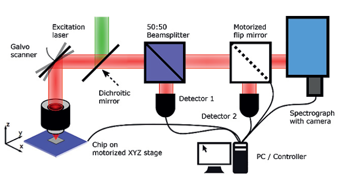
Figure 1: Confocal setup for automated device characterization: Excitation light (green) is directed over the dichroic mirror through the objective to the chip with photonic structures and emitter. The PL of the emitter is collected through the same objective, passes the dichroic mirror and is divided by the 50:50 beam splitter to detector 1 and the spectrograph. A flip mirror enables the analysis of the second order auto correlation function if inserted before the spectrometer.
Screening our chip with the automated setup, allows efficient pre-characterization of hundreds of devices. At each device position a PL scan is used to focus on the brightest spot and a spectrum is recorded with an acquisition time of 300 s. When the whole measurement is finished, the spectra are classified by the presence of resonances and the average intensity. An example measurement of three neighboring devices with the corresponding PL maps and spectra are presented in Figure 2. The first device (a) shows a pronounced peak at 665 nm and an intermediate intensity with about 1,000 counts, from which efficient optical coupling and a low number of emitters is inferred. The second device (b), also shows a weak resonance at 630 nm, but reaches almost twice the intensity, which excludes the presence of a single emitter. The third device (c) appears to be empty, since neither a resonance (only hot-pixles) nor a high signal is present. Only in the first case (a) a coupling between a single quantum emitter and a high Q cavity is measurable, so that it can be further investigated.
The single photon spectrum of an emitter-cavity system is a unique characteristic and enables classification of the coupling. In order to measure hundreds of devices we integrate the camera, combined with a spectrograph, in our single photon sensitive home-built setup and embed it in a customized software solution. Even though the PL signal is on the single photon level and the resonances are designed to have a linewidth of below a nanometer, the recorded spectra enable sufficient classification of the coupling with moderate integration time (5 min). The camera is an essential part of the automated setup and allows us to increase the throughput of quantum optic experiments.
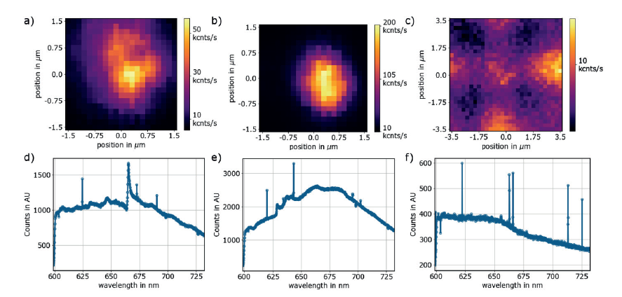
Figure 2: Photoluminescence maps a)-c) and spectra d)-f) of emitter-cavity devices from automated measurements: left: Single NV and cavity with resonance at 665 nm, center: two NV and cavity at 630 nm, right: No NV in cavity.
P. P. J. Schrinner, A. Eich, C. Schuck, Institute of Physics, Integrated Quantum Technology, University of Münster, Germany (June 2020)

© Oxford Instruments 2026
