Resources
 Part of the Oxford Instruments Group
Expand
Collapse
Part of the Oxford Instruments Group
Application Notes
Author: Dr. Assegid Mengistu Flatae, University of Siegen, Germany
Published: 01 Jul 2020 · Last updated: 24 May 2023
Electrically-driven solid-state single-photon sources operating at room temperature are crucial to the development of quantum technologies, such as quantum computers and secure communication lines. Electrically-driven semiconductor quantum dots currently exhibit the best performances, but they require operation at cryogenic temperatures [1]. Under ambient conditions, negatively charged silicon vacancy (SiV-) color centers in diamond represent an alternative platform as the fluorescence signal is concentrated in a narrow zero-phonon line and it exhibits a short excited-state lifetime [2].
The electrical excitation of SiV- color centers is determined by electron and hole-capture processes. This possibility has been recently demonstrated using p-i-n based diode structures, where the Si ions are implanted in the intrinsic layer [3]. However, the creation of SiV- color centers in p- or n-type diamond could avoid the need for complex semiconductor junctions. For example, SiV- color centers in n-type diamond would allow the implementation of a Schottky-diode.
However, to attain single-photon emission from SiV- color centers in n-type, e.g., phosphorous-doped (P-doped), diamond is challenging. Crystal imperfections (structural distortion and degradation caused by the incorporation of phosphorus atoms during the growth process), phosphorus-related complex defects, luminescence related to phosphorus-nitrogen co-doping and ion-beam induced defects can compromise the signal-to-noise ratio required for single-photon emission [4].
Here, we discuss the optical properties of SiV- color centers in P-doped single-crystal diamond implanted with Si ions. The optical characterization is based on a homemade µ-photoluminescence setup, as shown in Fig 1a. The sample is excited by a diode laser and the emission from the sample is collected via a microscope objective (Olympus, 50×, 0.95 NA). Imaging is performed under wide-field laser illumination and the collected signal is sent to a sCMOS camera (Zyla-4.2P-USB3-W, Andor Technology). Flippable mirrors give access to a spectrometer (QE Pro, Ocean Insight).
Unlike for intrinsic single-crystal diamond [1], P-doped diamond can exhibit a huge background at the emission wavelength of the SiV- color centers. In order to understand the origin of the background and optimize the signal-to-noise ratio of the SiV- color centers, we investigated the sample (single-crystal diamond grown by chemical vapour deposition with 4300 ppm phosphorus concentration, implanted with 108 to 1014 Si-ions/cm2 and annealed at high temperatures) using 532 nm (Thorlabs, CPS532 - Collimated Laser-Diode-Pumped DPSS Laser Module), 656 nm (PicoQuant, PDL 800-D, LDH-DC-660) and 690 nm (PicoQuant, PDL 800-D, LDH-DC-690) laser excitation. The background related to the nitrogen-vacancy (NV) color center (neutral and negatively charged states, NV0 and NV-, respectively) is evident in the spectra, when the sample is excited by the 532 nm laser. These features are strongly suppressed, when the excitation wavelength is 656 nm and 690 nm (see Fig 1b), as NV color centers have significantly less absorption in this spectral range. This is due to the formation of NV color centers and other defects as ion implantation creates vacancies and thermal annealing favors the formation of NV complexes in addition to the desired SiV- color centers. By reducing the nitrogen concentration in the technical gases during the growth of P-doped diamond, the luminescence background can be significantly suppressed even for high phosphorus doses and the conditions for single-photon emission can be attained [4].
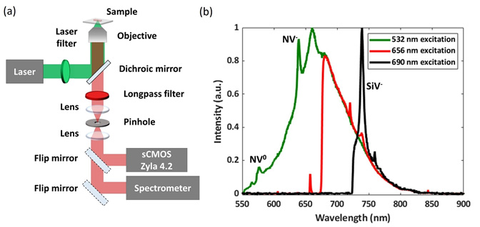
Figure 1. (a) Schematics of the µ-photoluminescence confocal microscopy setup. (b) Photoluminescence spectra of the P-doped diamond sample using 532 nm, 656 nm and 690 nm. The background due to NV color centers is reduced by choosing the 690 nm excitation wavelength, as NV complexes have less absorption in this spectral range. The labels refer to the zero-phonon lines of the NV0, NV-, and SiV-.
Next, in order to interrogate individual SiV- color centers in P-doped diamond, the sample is wide-field illuminated (~ 50 µm) using the 656 nm laser wavelength at a power of 9.61mW. The overall detection efficiency of the setup at the emission wavelength of the SiV- color centers (before the imaging camera) is around 1 %. This number takes into account light trapping inside diamond due to its large refractive index. In this wavelength range the Zyla-4.2 sCMOS imaging camera has a quantum efficiency QE of ~ 65 % (more than 80 % QE at the emission wavelength of NV color centers). Information about the counts, offset and sensitivity of the camera, allows to determine the photoelectrons generated on the sensor. Dividing this number by the QE of the sensor at 738 nm, determines the number of incoming photons (photon flux), as shown in Fig. 2.
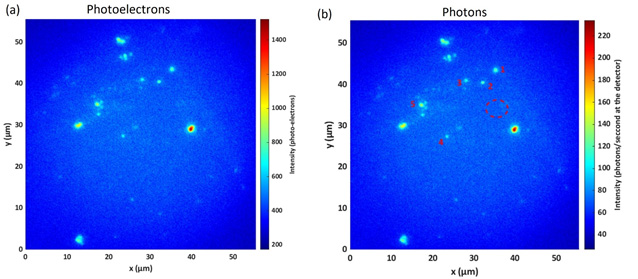
Figure 2. (a) Photoelectrons and (b) incoming photons on the Zyla 4.2 sCMOS camera. The photoluminescence is filtered with a 13 nm bandpass centered on the SiV- zero-phonon line.
The photon flux S (photons/second) is related to the signal-to-noise ratio (SNR) according to:
where B = 80 photons/s is the background taken where there are no emitters (see red circle in Fig. 2b), t = 10 s is the exposure time, QE = 0.65 is the quantum efficiency of the sensor at 738 nm, D = 0.019 electrons/s is the dark-count rate and r = 0.9 electrons/s is the read-noise at a readout speed of 216 MHz. Table 1 shows the photon flux and the SNR of 5 different SiV- color centers in the P-doped sample.
| SiV Color Center Mark | Photon Flux | SNR |
| 1 | 129 | 23 |
| 2 | 129 | 23 |
| 3 | 111 | 20 |
| 4 | 115 | 21 |
| 5 | 138 | 24 |
Table 1: The photon flux and the SNR of 5 different SiV color centers shown in Fig. 2b.
In order to use the Zyla 4.2 sCMOS camera for photon counting and determine the ultimate performance of the device for the detection of SiV- color centers in P-doped diamond samples, we determine the average SNR of the color centers as a function of acquisition time (exposure time). Figure 3 shows the SNR and the required exposure time for imaging low signal levels. The SNR value represents the ratio of the signal from SiV- color centers to the combined noise that consists of the sample fluorescence background, the sCMOS electronic noise and the photon shot noise. The latter is an inherent property of light that cannot be reduced by using other camera designs nor sensors, it represents the minimum achievable noise level. When the exposure time is small (the dark current is 0.019 electrons/s), the read noise is greater than the photon noise. So, the signal is mainly read-noise-limited and the SNR can be best described by
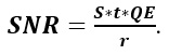
This corresponds to a region that has an acquisition time below ten ms, as shown in Fig. 3. The read noise mainly arises from the process of converting charge carriers into a voltage signal for quantification and subsequent processing. In the read-noise-limited region (see Fig. 3 shaded part), the SNR is too small to observe a detectable signal. The camera exposure time should be more than 200 ms to collect signal that has a SNR larger than 3, which in turn makes photon noise the dominant noise source. The SNR in this photon-noise-limited region is given by
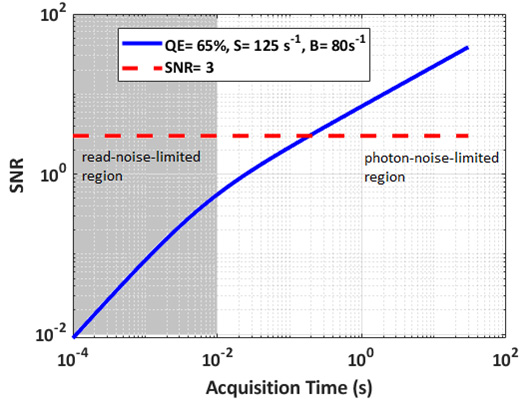
Figure 3: Double logarithmic plot of the signal to noise ratio of the average SNR (see Table 1) as a function of the acquisition time.
In conclusion, we discuss the optical properties of SiV- color centers in P-doped diamond and the imaging settings based on a Zyla-4.2 sCMOS camera. The high QE of the sCMOS sensor in the near infrared makes the color centers clearly observable with a moderate exposure time. Improvements in the collection efficiency and in the homemade setup can further reduce the acquisition time. Furthermore, the background (B) due to NV color centers can be further reduced by exciting the SiV- color centers at longer wavelengths (e.g., 690 nm) as NV complexes have less absorption.
The authors would like to acknowledge the contribution of S. Nicley, K. Haenen, R. Rechenberg and M. F. Becker for P-doped diamond growth, S. Lagomarsino, S. Sciortino, N. Gelli, L. Giuntini and F. Taccetti for diamond implantation and annealing and P. Reuschel, N. Soltani and D. Yu Fedyanin for helpful discussions. Financial support from the University of Siegen and the German Research Association (DFG) (INST 221/ 118-1 FUGG, 410405168) is gratefully acknowledged.

© Oxford Instruments 2026
