Resources
 Part of the Oxford Instruments Group
Expand
Collapse
Part of the Oxford Instruments Group
Application Notes
Author: R. H. Godiksen, A.G. Curto, Department of Applied Physics and Institute for Photonic Integration, Eindhoven University of Technology, Netherlands
Published: 01 Jun 2020 · Last updated: 04 May 2023
Due to the continuous need to improve information technologies, research into advanced materials with improved electronic properties is needed. Beyond the electron charge as the carrier for information processing, layered van der Waals materials now offer novel degrees of freedom such as the momentum direction (valley index)[1] or the layer number, that could be exploited as a resource for electronic and optoelectronic devices. The emerging field of valleytronics aims at information processing based on the momentum of carriers, rather than charge transport between two electrodes. Material requirements to make it possible are: having two or more valleys in the band structure (conduction and valence band extrema in different crystal directions), and the ability to controllably populate the valleys with charge carriers.
Two-dimensional semiconductors such as MoS2 or WS2 are promising materials for nanophotonics and optoelectronics [2-4]. Their valley properties are of particular interest because they are readily accessible through circularly polarized light. Due to inversion symmetry and spin-orbit coupling, these atomically thin semiconductors have optical selection rules enabling the excitation of carriers in either the K- or K’-valley of the hexagonal Brillouin zone by left- or right-handed circular polarized light [1]. However, both material composition and thickness affect the lifetime of a carrier in the excited valley, thus requiring studies into the properties for the most suitable valleytronic materials.
Polarization-resolved photoluminescence can be used to characterize valley polarization. Our setup is an epi-illuminated confocal microscope, with a circularly polarized excitation laser and circular polarization analysis in emission (Fig. 1). To analyze the spectral polarization dependence of the photoluminescence, we use a combination of an Andor Shamrock SR-303i-B-SIL spectrograph and a front-illuminated Andor Newton DU970P-FI electron-multiplying CCD camera. The Shamrock spectrograph allows us to record both spectra and decay lifetime thanks to its dual output ports. The Newton EMCCD camera, thanks to its electron multiplication gain and the thermoelectric cooling down to -80 ºC, allows us to detect photoluminescence with a wide range of intensities: from the bright emission of direct bandgap monolayers to the dim signal of indirect bandgap multilayers, all within the same experimental platform.
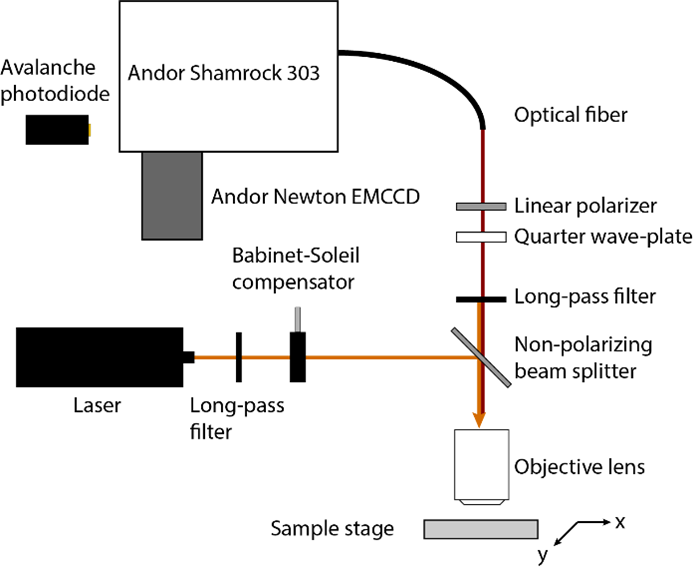
Figure 1. Schematic of the experimental setup for measuring valley polarization in layered semiconductors.
We exploit the ability to measure low light signals to study layered materials such as a bilayer WS2 (thickness around 1.4 nm), which has an indirect band gap with very low photoluminescence quantum yield. Keeping the excitation polarization fixed and switching between left- and right-handed circularly polarized light in the detection path, we measure a clear contrast in the circular polarization of the emitted light at room temperature in the range of 1.9-2 eV (Fig. 2). Moreover, the fast kinetic series measurement mode enables us to acquire spectra quickly, even for photoluminescence signals varying over time. We observe a high degree of circular polarization in bilayer WS2 at room temperature, in sharp contrast to most other two-dimensional semiconductors that require cryogenic temperatures to measure a similar degree of polarization. The low noise and the electron-multiplying gain capabilities of the Newton camera are important for an effective analysis of the spectral response for both polarizations, as the material quantum efficiency is low due to the indirect nature of the band gap.
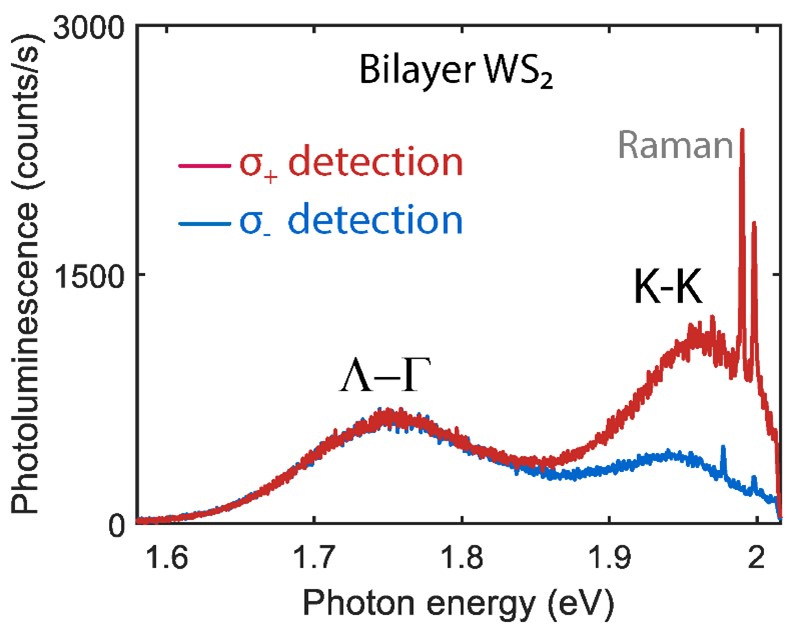
Figure 2. Photoluminescence spectrum from a bilayer WS2 excited by σ+ polarized light with a laser photon energy of 2.04 eV.
Dr. Alberto G. Curto
TU/e – Eindhoven University of Technology
Groene Loper 19
5612 AZ Eindhoven
The Netherlands
E-mail: A.G.Curto@TUe.nl
Web: http://www.Nano-Optics.nl

© Oxford Instruments 2026
