Resources
 Part of the Oxford Instruments Group
Expand
Collapse
 Part of the Oxford Instruments Group
Photovoltaic devices (PV) made from perovskite or organic materials have become very interesting in research over the last decade due to their intrinsic properties and their potential application in the growing market of renewable power generation. Although both device types have fundamental differences in terms of potential application, they share large scale low-temperature, low-cost fabrication. Perovskite solar cells [1, 2] are based on the ABX3-type with a structure made of an organic or inorganic cation A, a metal like Pb or Sn as central ion B, surrounded by the ligands X consisting of halogens or halogen mixtures. These materials behave like inorganic semiconductors with a band-to-band transition leading to free carrier formation. Single junction cells reach currently a power conversion efficiency close to 25 % [3, 4].
Organic solar cells are nearing 20 % power conversion efficiency [5] and work fundamentally differently, since the charge generation needs to overcome the substantial binding energy of the primary, optically-generated exciton. Our current interest in organic PV is due to indoor applications for the internet-of-things where organic materials easily surpass 20 % power conversion efficiency.
However, it is currently accepted knowledge that both types of devices are limited by open-circuit voltage (VOC), whereas short circuit density and fill factor are close to the theoretical limits. Thus, we are interested in pushing the limit of (VOC) since there is more potential to increase performance of current PV devices. Because the maximum (VOC) with a given band gap of the material [6] (or charge transfer state in organics [7]) is inherently linked to radiative recombination in solar cells [8], electroluminescence (EL) is a viable method [3, 4, 9] to investigate potential improvements. The challenge is, however, to detect a low number of photons in the near IR. The devices are driven at voltages close to the thermodynamic limit (i.e. band gap or VOC) and low currents. This causes, in some cases, low quantum yields in recombination being on the order of 10-5 to 10-3 as opposed to the best devices [3, 4].
In order to measure EL reliably, we use a fibre coupled Kymera 328i-B2-SIL spectrograph equipped with two 150 l/mm gratings blazed at 800 nm and 1450 nm. Attached on one exit port is an iDus InGaAs photo-diode array DU491A-1.7. The fibre is brought into contact with the transparent glass of the PV device which is driven by a Keithley SMU at a voltage as low as possible or in some cases at a short circuit current density corresponding to AM1.5 solar illumination (100 mWcm2). Data acquisition is done using the Andor Solis software.
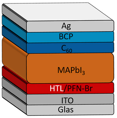
First, we take a closer look to the PVSK device. In Fig. 1 a typical device layout of a pin junction is depicted.

Figure 1: Sketch of the device architecture of a MAPbI3 (PVSK) single junction photovoltaic cell. ITO is the transparent electrode on a glass substrate, HTL is a hole transport layer covered with an interfacial layer made of the ionic polymer PFN-Br. The active absorbing and charge generating layer is the perovskite MAPbl3 covered with electron transport layer C60, blocking layer BCP and finally the back electrode made of silver (Ag). For the present experiment we varied the properties of the HTL layer.
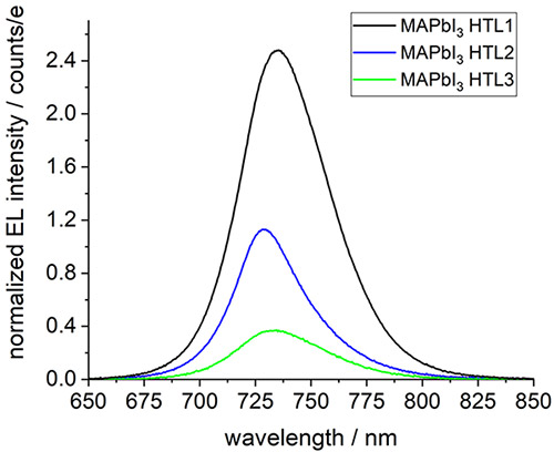
The total layer thickness is about 500 nm excluding the electrodes. Due to expected limitations of the device on the HTL/MAPbI3 interface we fabricated devices with three different HTLs keeping everything else constant. The devices have good PCE of 18 ± 0.5 %. The short circuit current and fill factor do not vary in a systematic way in these devices, however the VOC does, decreasing with decreasing PCE. The spread is about 50 mV, being 270 mV or 20 % short of the Shockley-Queisser limit. In order to show that the loss in VOC is related to non-radiative recombination we performed EL measurements. A comparison of relative EL efficiency of the three devices is shown in Fig. 2.

Figure 2: EL spectra normalized to the driving current density of three PVSK devices.
Besides a minor change in peak position of the EL spectrum the striking difference is a variation in intensity. The highest EL efficiency is obtained with the device with HTL1 showing also the maximum VOC. A loss of 50 mV in VOC results in an EL intensity loss of about a factor of six. Since our VOC is not close to the theoretical limit, the main loss is due to non-radiative recombination. Even taking into account higher interface recombination in MAPbI3/HTL3 compared to MAPbI3/ HTL1 the difference does not account for all losses. We conclude that a significant part of the non-radiative loss is due to volume recombination. A quantitative analysis would require a calibration of the spectrometer with an absolute standard, which is currently not feasible.
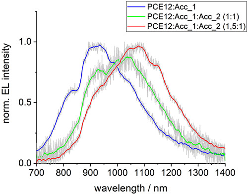
To exploit the sensitivity of our setup we used organic PV devices made of the donor polymer PCE12 with varying acceptors and varying composition. This should influence the charge-transfer state energy and hence, VOC [7]. In typical indoor light applications, the employed current densities are below 1 mA/cm2, which is a factor of 10 to 100 less compared to solar cells. Driving the device at around 1 V (close to VOC) results in very few emitted photons. The lower radiative efficiency of CT states of organic PV materials yields orders of magnitude less emission compared with the MAPbI3 investigation described above. The detector was cooled to 50 °C using the built-in thermoelectric cooler and the integration time increased to 0.5 s. Averaging over 50 acquisitions resulted in EL spectra shown in Fig. 3.

Figure 3: EL spectra normalized to peak intensity of three organic PV devices with varying acceptor composition. The coloured curves are smoothed averages of the raw data.
The EL spectra shift to lower energy with varying acceptor composition. The pure donor PCE12 compound and the pure acceptor compounds have EL spectra peaking in the red part of the visible (not shown), thus the emission originates from a different species. Most likely the combined donor:acceptor molecules form a charge transfer state with lower energy. The exact CT energy shows a broad distribution reflected in the broad EL spectra. However, the onset and the peak position scale with the obtained VOC. The lower the VOC the lower the emission energy in the PCE12:acceptor combination. The best PV device reaches a PCE of 23 % at 200 lux illumination being currently close to the state-of-the-art for organic PV.
In summary the challenging detection of extremely low EL emission of solar cells was measured with sufficient spectral resolution using the Kymera/iDus setup.
I would like to thank M. Neubauer, M.H. Fard and R. Bruker for fabrication of the PV devices used here.
[1] K. Jena et al., Chem. Rev. 2019, 119, 3036.
[2] Y. Kim et al., Chem. Rev. 2020, 120, 7867.
[3]Jeong et al., Nature 2021, 592, 381.
[4]J. Yoo et al., Nature 2021, 590, 587.
[5] https://www.nrel.gov/pv/cell-efficiency
[6] Shockley, H. J. Queisser, J. Appl. Phys. 2004, 32, 510.
[7] K Vandewal et , Nat. Mater. 2014, 13, 63.
[8] Rau, Phys. Rev. B 2007, 76, 085303.
[9] Tress et al., Adv. Energy Mater. 2015, 5, 1400812
Dr. Dirk Hertel Institute of Physical Chemistry
Department of Chemistry
University of Cologne
Greinstr. 4-6
50939 Cologne, Germany
Phone: + 49 (221) 470-2494
E-mail: dirk.hertel@uni-koeln.de
Web: https://chemie.uni-koeln.de/forschung/physikalische-chemie
