Resources
 Part of the Oxford Instruments Group
Expand
Collapse
 Part of the Oxford Instruments Group
Challenge Background
Nanotechnology is becoming ever-more pervasive in the world around us and the devices that we now depend on such as the sensors (motion, pressure, temperature), materials with exotic properties such as water proofing, extreme strength, ‘smart’, low stiction, display screen technology and so on, with an ever-increasing list of applications. With such small sizes on the nano- and micro-scale, materials take on special properties divergent from the bulk where quantum properties become highly significant. Examples of materials encountered are quantum dots and wires made of semiconductor material, carbon nanotubes, and plasmonic nanostructures [1,2]. Key to these developments is having a clear understanding of the underlying quantum properties. Among the key parameters for characterising these materials is their physical size, shape, crystal structure, chemical stoichiometry and, carrier density and transport. A range of tools are available which include AFM, SEM, SNOM, PSTM, TERS and Photoluminescence spectroscopy (PL).

Technology Solution
Photoluminescence is a powerful spectroscopy and imaging technique for elucidating properties of the charge carriers within these quantum structures. In semiconductor materials the bandgaps tend to lie in the NIR region so excitation of the sample with lasers in the NIR is of particular of importance, giving rise to near-infrared photoluminescence (NIR-PL) studies in the spectral region from ~700 nm up to ~2 µm. The main components required for the experiment will be an excitation source usually a laser, sample holders and delivery/collection optics often in a micro-spectroscopy configuration, a dispersive spectrometer and a high-sensitivity detector. The latter is of key importance as one is often dealing with low photon regimes – especially if experiment is looking at single particles. As an illustrative example, excitation of at 950 nm has been used to investigate the attractive and repulsive Coulomb interactions among electrons and holes confined to one dimension within InAs/InP QWRs by monitoring the photoluminescence emission at 1.5 µm [1]. This offers information on how the electronic and optical properties change with the density of trapped carriers
Andor Solutions
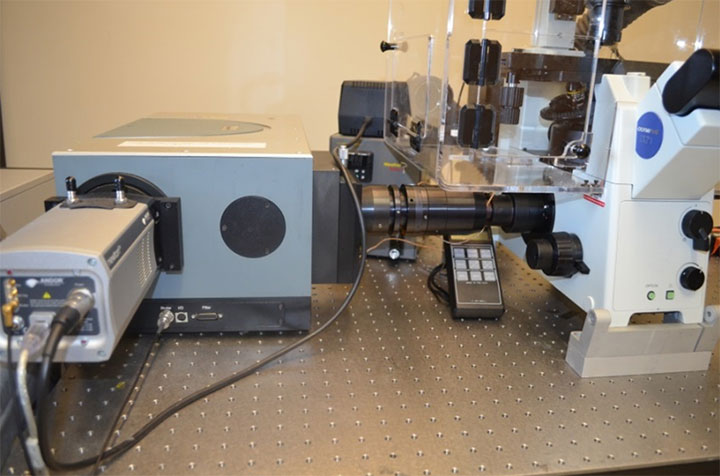
Andor provides a range of highly sensitive detectors for the NIR along with the Kymera and Shamrock series of spectrometers, covering the spectral range from visible through NIR to beyond 1.7 µm. Silicon based detectors have sensitivity up to just beyond 1 µm. The InGaAs based detectors provide sensitivity to the longer wavelengths of 1.7 µm and 2.2. µm depending on the material used. There are several key sensor technologies to be borne in mind when choosing a detector in the NIR:
| Key Requirement | NIR-PL Solution |
| Efficient detection in NIR up to ~1 µm – with FST, and high QE | iDus, Newton, iVac and iKon families: Sensor types for NIR region: -BR-DD, BEX2-DD, LDC-DD |
| Detection up to 1.7 µm or 2.2 µm | iDus-InGaAs series: DU490A-1.7, DU491A-1.7, DU490A-2.2 |
| Dispersion with good resolution, high throughput, wide bandpass | Spectrometers – Kymera and Shamrock series: KY193i, KY328i, SR500i, SR750 |
References
