Resources
 Part of the Oxford Instruments Group
Expand
Collapse
Part of the Oxford Instruments Group
Expert Insights
Author: Dr. Shayne Harrel
Published: 01 Apr 2023 · Last updated: 02 May 2023
Atomic spectroscopy involves the interaction of atoms with light, while molecular spectroscopy involves the interaction of molecules with light. Atomic spectroscopy provides information about the atomic or elemental identity of a sample, while molecular spectroscopy can reveal information about molecular identity and molecular structure.
The types of transitions involved atomic vs. molecular spectroscopy are different: in atomic spectroscopy electronic state transitions are typically observed, while in molecular spectroscopy, in addition to electronic state transitions, vibrational and rotational transitions can also be studied. This article focuses on molecular spectroscopy. You can view our other articles for a in depth description of atomic spectroscopy.
Spectroscopy experiments are reported in different units, depending on the technique being used. Figure 1 identifies some key regions in the electromagnetic (EM) spectrum, some common spectroscopy techniques used in these regions, the type of transitions probed by each technique and the units used.1 For example, UV-Vis absorption spectroscopy involves transitions with valence electrons in molecules ad is reported in units of wavelength (λ) such as nanometers (nm) or angstroms (Å). Infrared absorption spectroscopy examines molecular vibrations and is reported in typically reported in wavenumbers (cm-1).
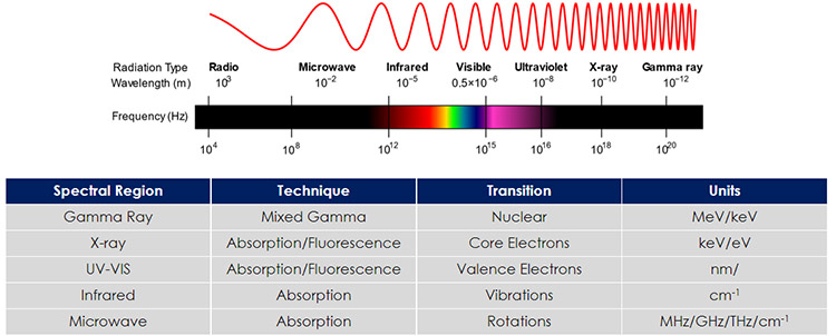
Figure 1: The electromagnetic spectrum (EM), spectroscopy techniques used, transitions involved and spectroscopy units. EM image taken from Reference 1.
Absorption spectroscopy is the absorption of EM radiation as a function the frequency of radiation due to its interaction with matter. Imagine having a sample in a cuvette interact with different types of light as shown in Figure 2. When the sample absorbs different types of light, different types of transitions are exited in the sample. With x-rays, transitions involving core electrons are excited. With UV-Vis light, valence electrons are excited. IR radiation excites molecular vibrations, and molecular rotations are excited in the microwave region. In the radio frequency (RF), electron and nuclear are excited.
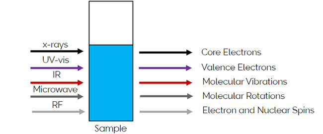
Figure 2: The different types of transitions in excited molecules based on the type of light used.
UV-Vis absorption spectroscopy in molecules involves exciting valence electrons between molecular orbitals. Two significant molecular orbitals are the highest occupied molecular orbital (HOMO) and the lowest occupied molecular orbital (LUMO). For a molecule in the ground electronic state, the HOMO is populated with electrons while the LUMO is not. In a UV-Vis absorption experiment, an electron is excited from the HOMO to the LUMO. Vibrational and rotational transitions can also occur when exciting from the ground to excited electronic state.
UV-Vis absorption spectrometers consist of a broadband light source, a dispersion element, a wavelength selector, a detector and a recorder as shown in Figure 3.2
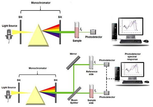
Figure 3: Single beam (top) and dual beam (bottom) UV-Vis spectrometers. Figure taken from Reference 2.
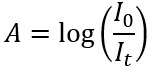
In a UV-Vis experiment, the absorbance of a sample, A, is calculated by taking the log of the ratio of the intensity of light that passes through a reference sample as a function of wavelength divided by the intensity of light that passes through a sample of interest as a function of wavelength:
This can be used to calculate the concentration of an absorbing species in a sample using the Beer-Lambert Law, or Beer’s Law:
Where ε is the molar absorption coefficient and is a measure of how strongly the absorbing species in the sample absorbs light having and is typically reported as M-1cm-1. c is the concentration of the absorbing species with units of molarity M, and d is the distance (sometimes called pathlength) that the light interacts with the sample. Beer’s Law works best when the absorbance is between 0.2-0.8. Dual-beam UV-Vis spectrometers make this measurement more convenient by using a beam splitter to excite both the reference and the sample at the same time. This allows the intensities of the reference and the sample to be collected simultaneously.
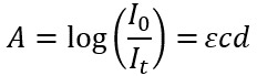
One example of Beer’s Law is using it to measure protein concentrations in a sample, such as those found in recombinant protein production. Proteins contain amino acids such as phenylalanine, tryptophan and tyrosine that have aromatic groups that absorb strongly in the UV. By measuring the absorption of a sample at 280 nm and applying Beer’s Law, the concentration of proteins can be estimated as shown in Figure 4.3 While this method may not be the most accurate due to the UV absorption of nucleic acid materials, which are often present in these sample types, combined the fact that different proteins will have these amino acids present in different ratios, it can be useful in monitoring protein purification in recombinant protein products. Commercially available instrumentation for purification, such as HPLC systems, often use UV-Vis based detection.
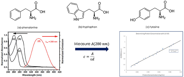
Figure 4: Three amino acids used in quantifying protein concentrations by UV-Vis spectroscopy. The plot on the left shows the UV-Vis absorption spectrum of (a) phenylalanine, (b) tryptophan, (c) tyrosine. The plot on the right shows the absorbance at 280 nm as a function of protein concentration obtained by Beer’s Law. UV-Vis absorption spectra obtained from Reference 3.
Photoluminescence is light emission from matter after the absorption of photons. There are two types: fluorescence and phosphorescence. Fluorescence is relatively intense and fast, with timescales on the order of picoseconds (ps) to nanoseconds (ns). In contrast, phosphorescence is weaker and slower, with timescales on the order of microseconds (μs) or longer. Both fluorescence and phosphorescence are redshifted compared to the excitation wavelength.
The Jablonski diagram, named after Aleksander Jabłoński, is a helpful tool for understand the different types of photophysical processes in molecules and is shown in Figure 5.4 This diagram describes the ground and excited electronic states of molecules, vibrational and rotational levels within both the ground and excited electronic states, the electron spin properties of these states, and the types of possible transitions between all of these states.
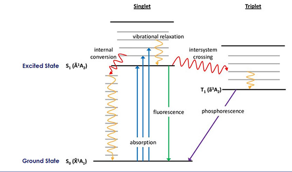
Figure 5: The Jablonski diagram which depicts possible photophysical processes in molecules. Image taken from Reference 4.
Fluorescence occurs when an electron in an excited electronic state relaxes to the ground electronic state by emitting a photon. This happens when both the ground and excited states are singlet spin states.
What can also happen is that an electronically excited electron in a singlet state can undergo an intersystem crossing (IC) into an electronically excited triplet spin state. The relaxation of an electron in an excited triplet state to a ground state by direct photon emission is quantum mechanically forbidden. However, this type of transition can and does happen due to spin-orbit coupling, and this process is the origin of phosphorescence.
A schematic diagram of a fluorescence spectrometer is shown in Figure 6.5 A light source, which can be either a broadband light source or a narrow-band laser, is focused by a lens onto a sample where electrons in the sample are excited from the ground state to the excited state. When the electron relaxes from the excited state to the ground state by emitting a photon, the emitted fluorescence is collected by placing a lens, usually at a 90o angle from the excitation path to minimize the background from the excitation source, and focused into a monochromator where it is detected. The data is then sent to a recorder, where the measured fluorescence is reported as the intensity of the light emitted as a function of the wavelength of the emission.
Figure 6: Schematic diagram of a fluorescence spectrometer. Image taken from Reference 5.
As an example, consider the absorbance and fluorescence spectrum of fluorescein shown in Figure 7.6 Fluorescein is a dye that is used for biological imaging. The absorption spectrum is shown in blue, and the fluorescence spectrum is shown in red. It is seen that the florescence spectrum is redshifted with respect to the absorption spectrum. This is called the Stokes shift. The fluorescence spectrum also looks like the inverse of the absorption spectrum, which is common in fluorescence experiments.
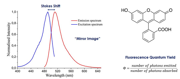
Figure 7: Absorption (blue) and fluorescence (red) spectrum of fluorescein. The fluorescence spectrum is redshifted from and appears as a “mirror image” of the absorption spectrum. Spectrum taken from Reference 6.
An important quantity in fluorescence measurements is the fluorescence quantum yield, Φ, which is the number photons a molecule emits divided by the number of photons a molecule absorbs:
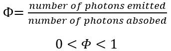
The maximum value of Φ is 1 where the molecule emits one photon for every photon absorbed, and the minimum value is 0 where the molecule doesn’t emit any photons.
It is possible to perform time-resolved fluorescence measurements with a pulsed laser and a time-resolved detection scheme. Near-Infrared fluorescent proteins (iRFP) are a class of genetically engineered fluorescent probes in biological imaging. Steady-state absorption and fluorescence spectra for several iRFPs are shown in Figure 8.7
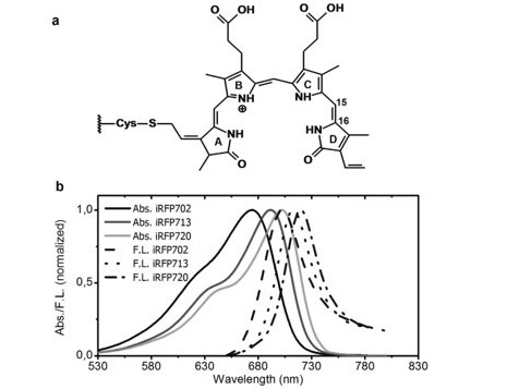
Figure 8: Left-steady state fluorescence spectra of near-infrared fluorescent proteins. Taken from Reference 7.
These proteins absorb and fluoresce toward the NIR, making them particularly useful for deep tissue imaging because light at longer wavelengths can travel further through tissue than light at shorter wavelengths. The time-resolved fluorescence spectra of iRFP702 at 702 nm following excitation at 660 nm in H2O and D2O is shown in Figure 9.7
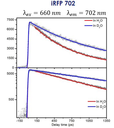
Figure 9: Time-dependent fluorescence spectra of iRFP 702 exited at 660 nm and detected at 702 nm in H2O (red) and D2O showing the kinetic isotope effect. The bottom trace is the same decay curve but on a logarithmic scale intensity. Taken from Reference 7.
It can be seen that the fluorescence intensity decays over time in the order of several hundreds of picoseconds (ps) to a few nanoseconds (ns). This time-dependent fluorescence intensity can be described as:
Where I(t) is the intensity of the fluorescence at a time, t, after excitation, Io is the initial intensity of the fluorescence and τ is the fluorescence lifetime which is the time it takes for I(t) to reach an intensity that is 1⁄e of the initial value (Io).
The fluorescence lifetime for iRFP 702 is different for the two solvents used here. In H2O, the fluorescence lifetime is measured to be 749 ps, while in D2O it is 1.35 ns. The longer fluorescence lifetime in D2O vs. H2O can be explained due to the presence of the heavier D isotopes, resulting in a Kinetic Isotope Effect (KIE) of 1.8 for the fluorescence lifetime of iRFP702 in these two solvents.
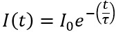
Förster Resonance Energy Transfer (FRET) is a process that can occur in fluorescence between two fluorophores. In FRET, two fluorophores are placed in close proximity to one another where the emission spectrum of one of the fluorophores (the FRET donor) overlaps with the absorption spectrum of the other fluorophore (the FRET acceptor), forming a FRET pair. When the donor molecule is excited from the ground to the excited electronic state, there can be a non-radiative energy transfer where the donor excites the acceptor, which then fluoresces as shown in Figure 10.8
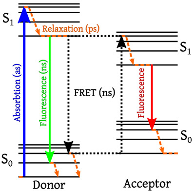
Figure 10: Jablonski diagram showing Förster Resonance Energy Transfer between a FRET pair. Image taken from Reference 8.
The efficiency of FRET is highly distance dependent, scaling as 1/r6 , where r is the distance between the donor and acceptor. Because of strong distance dependence, FRET only occurs when the donor and acceptor are a few nanometers apart and has applications in super-resolution localization imaging as well as in detecting and tracking protein interactions.
Phosphorescence is widely being used to characterize “next generation” materials like nanomaterials, low-D materials, and novel-type semiconductors. Many of these materials have applications in photovoltaics, energy generation and solar cells. The setup for a phosphorescence experiment is very similar to that of a fluorescence experiment, as schematically shown in Figure 11.
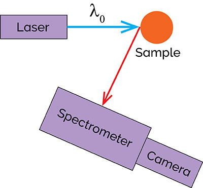
Figure 11: Schematic diagram of a phosphorescence spectrometer.
Gallium nitride nanostructures are one example of a next generation material and have gained interest because the phosphorescence from these nanostructured semiconductors emits in the blue, making them a candidate for use in blue LED and diode-based lasers. Phosphorescence was used to characterize the quality of gallium nitride nanostructures as shown in Figure 12.9 By using an xy translation stage, the researchers were able to generate a map of the overall intensity of the phosphorescence as well as identify the imperfections in the nanostructures by monitoring the presence or absence of a defect band at 370 nm, in addition to the normal phosphorescence emission at 360 nm.
Figure 12: Bottom left-PL total intensity from GaN based nanostructure arrays as a function xy position. Bottom right-representative PL spectra of GaN based nanstructure array showing the main PL emission at ~360 nm and detect band at ~370 nm. Adapted from Reference 9.
Researchers have been searching for alternative materials in place of traditional crystalline Silicon to use as thin-film absorption layers in thin-film solar panels to reduce production costs and improve sustainability. Copper Zinc Tin Sulfide (CZTSSe) has been identified as a viable and particularly attractive candidate for this because is it composed only abundant materials with low toxicity. Quantitative phosphorescence can be used to gain information about the electronic structure of these materials, which can be used to predict what the open circuit voltage would be when using such a material in a device. This is important because these measurements can be made early on in a production process and a whole solar cell device doesn’t have to be fabricated to gain this information.
In the experiment shown in Figure 13,10-12 researchers were able to alter the electronic properties of CZTSSe by introducing a layer of a semiconducting material, called a buffer, and monitor the effect of these changes using quantitative phosphorescence. The effects of using several buffers on the intensity of the phosphorescence just below 1.05 eV was used to ultimately predict how the material will perform in a device depending on the buffer used.
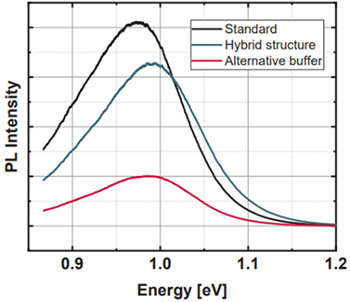
Figure 13: Bottom-PL spectra measured on Copper Zinc Tin Sulfide (CZTSSe) absorbers with several buffers. Adapted from References 10-12.
Raman spectroscopy can be used as a highly sensitive probe of molecular vibrations and rotations. It was first discovered by the Indian physicist, C.V. Raman, who published his results in a 1928 Nature paper titled “The Negative Absorption of Radiation”. In contrast to infrared absorption spectroscopy, which probes molecular vibrations and rotations by direct absorption of IR light having energy equal to the vibrational and rotational transitions in a molecule, Raman spectroscopy work differently. In a Raman experiment, an excitation source that is not resonant with any of the vibrational or rotational states in a molecule is used to excite electrons in a molecule to electronic virtual states, which results in scattering events. The most common scattering event is Rayleigh scattering, where photons scatter elastically with the molecule and the energy of these photons is not changed after the event. However, the photons can inelastically scatter with the molecule, where the energy of the photon after the scattering event is reduced by an amount equal to a vibrational or rotational level in a molecule - this is known as Stokes Raman scattering. Also, a photon can scatter inelastically with a molecule and gain energy after the event, where the energy gained is equal to a vibrational or rotational level in a molecule. This is known an anti-Stokes scattering. Both Stokes and anti-Stokes scattering are relatively inefficient, with only about 1 in 10-7 photons being inelastically scattered. These different processes are shown in Figure 14.13
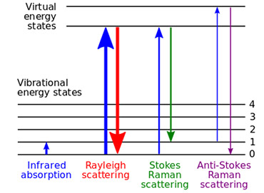
Figure 14: Energy levels and scattering events in Raman spectroscopy. Taken from Reference 13.
Figure 1514 shows a schematic setup for a Raman. Light is used to excite the sample and the resulting scatter is passed through a filter to reduce the intensity of the Rayleigh scatter. The light then enters a spectrograph where it is dispersed and collected with a detector and recorded.
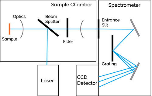
Figure 15: Schematic diagram of a Raman spectrometer. Taken from Reference 14.
The units typically used in Raman spectroscopy are wavenumbers (cm-1). However, what is unique to Raman spectroscopy is that the units corresponding to vibrational or rotational transitions in a sample are always reported relative to the energy of the excitation source, or Rayleigh line. For example, suppose an unknown Raman band is observed at 457.4 nm when exciting at 435.83 nm. Based on the equation:

Where h is Plank’s constant, c is the speed of light and λ is the wavelength of light, the energy of the excitation source is:

while the energy of inelastically scattered light is:

This results in an energy of 1082 cm-1 for the transition giving rise the unknown band at 457.4 nm:

The Raman signal is based on scattering events, which scale inversely with the fourth power of the excitation wavelength, 1/λ4 , so using a lower wavelength excitation source can increase the intensity of the Raman signal. The Raman “spectral density”, i.e., how close Raman modes at a given energy are to one another in wavelength space, depends highly on the wavelength of the excitation sources and the region of the spectrum of the modes are being studied. For example, consider an experiment where the goal is to measure molecular vibrations and rotations having energies ranging from 0 to 4000 cm-1 using Raman spectroscopy. If the excitation source was chosen to be at 262 nm, then the highest energy mode at 4000 cm-1 would appear at 292.7 nm, or ~30 nm redshifted from the excitation source. However, if the excitation source was chosen to be 785 nm, then this same mode at 4000 cm-1 would appear at 1144 nm, redshifted nearly 360 nm from the excitation source. This spectral density dependence on the wavelength of the excitation source requires that the spectral bandpass and resolution of a spectrograph and the wavelength dependent quantum efficiency of the detector being used should be carefully considered when designing a Raman experiment.
Raman spectroscopy is a non-destructive technique that is highly specific, and this specificity can be used to characterize materials in many ways. It can be used as a way of identifying unknown chemicals such as hexachlorobenzene as seen in Figure 16.15
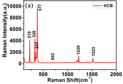
Figure 16: The Raman spectrum of hexachlorobenzene. Taken from Reference 15.
It can also be used as a means of quantifying the chemical composition of transition-metal dichalcogenide (TMDC) type monolayers such as MoS2 and WS2, by measuring the mole fraction of Mo with respect to W in Mo1-xWxS2 monolayer alloys as shown in Figure 17.16
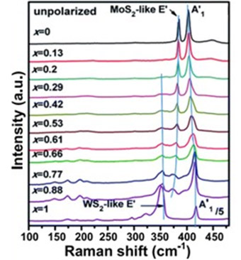
Figure 17: Raman spectra of Mo1-xWxS2 monolayer alloys as a function of W to Mo mole fraction. Taken from Reference 16.
The growth of multilayer nanomaterials can also be monitored by looking at the evolution of Raman modes as a function of layer number in MoS2 as seen in Figure 18.17 As the number of layers in the material is increased from 1 to 4, there are additional modes that appear in the Raman spectrum attributed to breathing and shearing modes in this material. These modes involve motions between multiple layers and the effect a motion on one layer has on another layer. Such multilayer dependent motions are only possible in a sample having multiple layers and are not present in the single layer Raman spectrum.
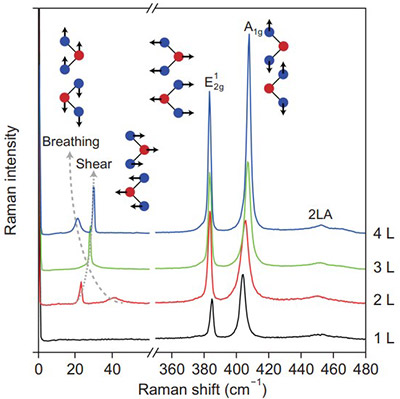
Figure 18: Raman spectra of MoS2 as a function of layer number. Additional Raman modes become apparent as the number of layers is increased. Taken from Reference 17.
Differences in molecular structure, such as those in water and ice, may also be characterized by Raman spectroscopy. While the chemical composition of water and ice is the same, the O-H stretching band in the Raman spectrum of water is much broader than in ice as seen in Figure 19,18 reflecting the fact that the OH group in water is free to explore more vibrational and rotational subspaces than in ice, where it is more confined.
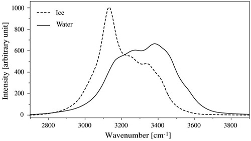
Figure 19: Raman spectra of water and ice showing the dependence of the line shape of the OH stretching mode in the liquid phase vs. solid phase. Taken from Reference 18.
Raman spectroscopy can be used to measure strain and defects in materials. Figure 20 compares the Raman spectrum of graphite in pure form to graphite samples that have been subject to extended periods of ball milling.19 The 2D band seen in graphite has a two peak profile which is supressed and transformed into a single peak, “bump-like” mode after 24 hours of milling.
Subtle differences in Raman spectral features can used to distinguish very similar materials, such as graphene and graphite. Graphene is a single layer of atoms arranged in a hexagonal lattice nanostructure, while graphite is composed of multiple stacked layers of graphene. Raman spectra of N-doped graphene and highly oriented pyrolytic graphite (HOPG) are shown in Figure 21.20 The 2D-band in N-doped graphene is slightly redshifted compared to the 2D-bank graphite. Furthermore, there are multiple modes that contribute to the 2D band in graphite resulting in a different line shape than what is seen in graphene. This difference is due to the multiple layers of graphene present in graphite. The D band seen in N-doped graphene is known as the defect or disorder band and is attributed to nitrogen doping of the sample.
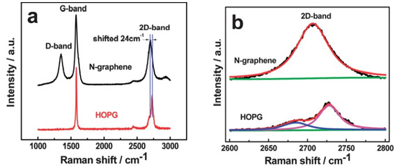
Figure 21: (a): Raman spectra of N-doped graphene (top) and highly oriented pyrolytic graphite (HOPG) (bottom). (b): Expanded view of the 2D-band in N-doped graphene and HOPG showing the fi difference in the line shape for the two materials. Taken from Reference 20.
Metallic and semi-conducting single-walled carbon nanotubes (SWCNT) can also be differentiated by Raman spectroscopy. The top trace in Figure 22 shows a Raman spectrum obtained on a metallic SWCNT while the bottom trace displays a Raman spectrum for a semiconducting SWCNT.21 The broadening of the G mode in the spectrum of the metallic sample compared to the semiconducting sample is used to differentiate two types of SWCNTs.22
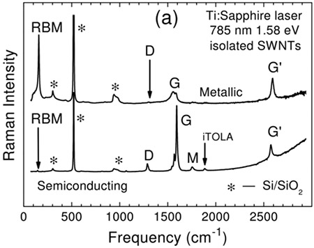
Figure 22: Raman spectra of metallic (top) and semiconducting single walled carbon nanotubes (SWCNT). Differences in the Raman spectrum such as broadening of the G band can be used to differentiate between metallic and semiconducting types of samples. Taken from Reference 21.
1. https://commons.wikimedia.org/wiki/File:EM_Spectrum_Properties_edit.svg
2. Sergio Braga, Mauro & Gomes, Osmar & Jaimes, Ruth & Braga, Edmilson & Borysow, Walter & Salcedo, Walter. (2019). Multispectral colorimetric portable system for detecting metal ions in liquid media. 1-6. 10.1109/INSCIT.2019.8868861.
3. Mahalingam, Venkataramanan & Hazra, Chanchal & Samanta, Tuhin. (2014). A Resonance Energy Transfer Approach for the Selective Detection of Aromatic Amino Acids. J. Mater. Chem. C. 2. 10.1039/C4TC01954G.
4. Ernest, Cheryl. (2011). High-Resolution Studies of the ùA₂– X̃¹A₁Electronic Transition of Formaldehyde: Spectroscopy and Photochemistry.
5. Li, Changzheng & Yue, Yanan. (2014). Fluorescence spectroscopy of graphene quantum dots: Temperature effect at different excitation wavelengths. Nanotechnology. 25. 435703. 10.1088/0957-4484/25/43/435703.
6. Bennet, Mathieu. (2011). MULTI-PARAMETER QUANTITATIVE MAPPING OF MICROFLUIDIC DEVICES.
7. Zhu J, Shcherbakova DM, Hontani Y, Verkhusha VV, Kennis JT. Ultrafast excited-state dynamics and fluorescence deactivation of near-infrared fluorescent proteins engineered from bacteriophytochromes. Scientific Reports. 2015 Aug;5:12840. DOI: 10.1038/srep12840. PMID: 26246319; PMCID: PMC4526943.
9. J. Malindretos, C. Hilbrunner, A. Rizzi, IV. Physikalisches Institut, Festkörper und Nanostrukturen, Georg-August-Universität Göttingen, Germany (April 2019).
10. David Regesch, Levent Gütay, […], and Susanne Siebentritt, Appl. Phys. Lett. 101, 112108 (2012), Degradation and passivation of CuInSe2.
11. Levent Gütay, David Regesch, […], and Susanne Siebentritt, Appl. Phys. Lett. 99, 151912 (2011), Influence of copper excess on the absorber quality of CuInSe2.
12. Thomas Unold, Levent Gütay, Wiley, Book chapter 11: Photoluminescence Analysis of Thin‐Film Solar Cells, Book: Advanced Characterization Techniques for Thin Film Solar Cells.
14. Schmid, Thomas & Dariz, Petra. (2019). Raman Microspectroscopic Imaging of Binder Remnants in Historical Mortars Reveals Processing Conditions. Heritage. 2. 1662-1683. 10.3390/heritage2020102.
15. Zhang, Xian & Zhou, Qin & Huang, Yu & Li, Zhengcao & Zhang, Zhengjun. (2011). Contrastive Analysis of the Raman Spectra of Polychlorinated Benzene: Hexachlorobenzene and Benzene. Sensors (Basel, Switzerland). 11. 11510-5. 10.3390/s111211510.
16. Chen, Yanfeng & Dumcenco, Dumitru & Zhu, Yiming & Zhang, Xin & Mao, Nannan & Feng, Qingliang & Zhang, Mei & Zhang, Jin & Tan, Ping-Heng & Huang, ying-sheng & Xie, Liming. (2014). Composition-dependent Raman modes of Mo1−xWxS2 monolayer alloys. Nanoscale. 6. 10.1039/c3nr05630a.
17. Lee, Changgu & Yan, Hugen & Brus, Louis & Heinz, Tony & Hone, James & Ryu, Sunmin. (2010). Anomalous Lattice Vibrations of Single- and Few-Layer MoS2. ACS nano. 4. 2695-700. 10.1021/nn1003937.
18. Claverie, Rémy & Fontana, Marc & Durickovic, Ivana & Bourson, Patrice & Marchetti, Mario & Chassot, Jean-Marie. (2010). Optical Sensor for Characterizing the Phase Transition in Salted Solutions. Sensors (Basel, Switzerland). 10. 3815-23. 10.3390/s100403815.
19. Kaniyoor, Adarsh & Sundara, Ramaprabhu. (2012). A Raman spectroscopic investigation of graphite oxide derived graphene. AIP Advances. 2. 032183-032183. 10.1063/1.4756995.
20. He, Chunyong & Li, Zesheng & Cai, Maolin & Cai, Mei & Wang, Jian-Qiang & Tian, Zhiqun & Zhang, Xin & Shen, Pei. (2012). A strategy for mass production of self-assembled nitrogen-doped graphene as catalytic materials. J. Mater. Chem. A. 1. 1401-1406. 10.1039/C2TA00807F.
21. Dresselhaus, M.S., Dresselhaus, A.G., & Jorio, A. (2007). Raman Spectroscopy of Carbon Nanotubes in 1997 and 2007. Journal of Physical Chemistry C, 111, 17887-17893.
22. Tambraparni, Bindu & Wang, Shiren. (2010). Separation of Metallic and Semiconducting Carbon Nanotubes. Recent patents on nanotechnology. 4. 1-9. 10.2174/187221010790712084.

© Oxford Instruments 2026
