Resources
 Part of the Oxford Instruments Group
Expand
Collapse
Part of the Oxford Instruments Group
Application Notes
Author: Dr Andrew Dennis
Published: 01 Aug 2022 · Last updated: 10 Aug 2022
CCD stands for Charge Coupled Device. There is also a variant called an EMCCD, and we have more detail on that in another article What is an EMCCD? The generic structure is basically the same as the CCD, but he EMCCD has one additional piece of circuitry, which does electron multiplication. So, they are EMCCDs, or electron multiplication CCDs.
Now, CCDs or EMCCDs are available in different types, which have different structures and layouts. These are front illumination, open electrode, back illumination, and deep depletion. And the following article will explain the differences between all these different types of CCD. We will also discuss anti-reflective coatings and how they work.
First let's discuss the structure of the pixel. The sub-element of the sensor, which is the part which responds to light, and converts photons into electrons.
In Figure 1 we have a very basic example of a CCD sensor. It's got 16 pixels, and it's what we're going to use to demonstrate the various types of structure of a sensor. So, within this 4 by 4 array of pixels, I've highlighted one individual pixel, and the individual pixel is made up of some building blocks. An electrode structure, shown here in blue, but it is in effect a network of wires across the front of the sensor.
![]()
Figure 1: The components of a Front-Illuminated CCD.
We've also got the depleted region; this is a region underneath the electrode, which is part of the sensor which responds to light. It's the part of the sensor that when electricity is applied to it, by the electrode structure, if photons shine on that depleted region, they will be turned into electrons, and they will be trapped in that region until the time comes to read them out. Underneath the depleted region is the bulk silicon, it's just the rest of the wafer. It's required to give substance to the sensor because the depleted region is particularly thin, and a thicker substrate is required.
Figure 2 gives a closer look at the electrode structure which are a network of wires. The incoming light must pass through this electrode structure before it hits the depleted region. So, in a standard front-illuminated sensor, which we call a front-illuminated sensor or FI sensor, the incident photons come from the sample. They're focused down on the sensor, and they must pass through this electrode structure.
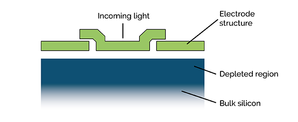
Figure 2: The CCD electrode.
The result of this is that the electrode structure blocks quite a lot of the light. The maximum sensitivity of a front-illuminated sensor is about 50%. And the terminology we use to describe this is quantum efficiency or QE. This is just the efficiency of the sensor to detect light. One hundred percent quantum efficiency means 100% of the photons at any one particular wavelength will be detected by the camera. And 50% quantum efficiency means half of the light will be detected by the sensor. The other half of the light will be reflected off or absorbed by the electrons, or somehow not measured. It might even pass right through the entire sensor.
Looking at the front illuminated design this you might say, "That's a terrible design." You've made this sensor, which can respond to light and turn the photons into electrons, so they can be measured later. But then you've covered the surface of your detector in wires, this electrode structure that blocks most of the light. But this is the fundamental initial type of CCD that was ever developed. This was the only real way that these sensors could be fabricated.
It's still a very cost-effective way of making CCD detectors. And a lot of researchers don't need really high sensitivity. If budgets do not permit the purchase of a very sensitive camera, a front-illuminated sensor will be good enough for a lot of applications, but there are ways to improve this, but they usually cost a little bit more, but let's consider the first variant of a CCD where we can modify the structure to give increased sensitivity.
An open electrode CCD is still front-illuminated because the light is passing through the electrode structure. The only thing that we've done here is modify the electrode structure as shown in Figure 3. For the sake of this schematic, I'm showing big holes in the electrode structure, so that more light can get through. It's not quite that straightforward, but it's a pretty good analogy.
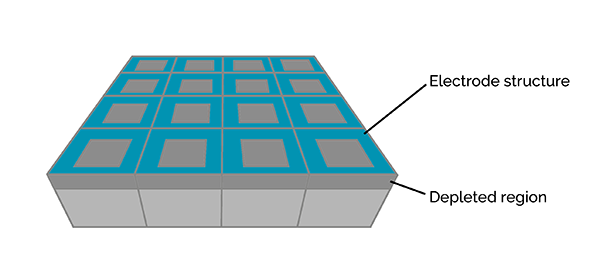
Figure 3: Open electrode CCD.
By having a change in the structure of the electrode, in this example, shown as holes in the electrode structure, you can get a considerable improvement in sensitivity across the spectrum. So, overall, the open nature of the electrode increases the ability to detect photons and, therefore, gives an improvement in sensitivity. It's a popular sensor for quite a lot of applications and is still quite cost-effective.
However, the electrode structure is there. The electrode structure is still blocking a large proportion of the light. And any sensible person would ask the question, can we not remove these electrodes? The fact is that we cannot remove the electrodes. They're a fundamental requirement of a CCD detector. But we can hide the electrodes as discussed in the next section on back-illuminated CCDs.
A back-illuminated CCD is the most sensitive type of CCD. Counter intuitively the manufacturing process starts with a front-illuminated CCD. First, we're going to flip it upside down, so we expose the back surface. Now, we've got the electrode structure right at the bottom and the depleted region. So, you're thinking, great, now the electrode structure is out of the way. Light's going to come in from the top down here, but now it hits this bulk silicon. And bulk silicon looks like metal. It looks like a standard piece of metal. It's shiny and sort of gray. So, now we've got the electrode structure out of the way, but the bulk silicon is going to cause a problem.
If we remove the bulk silicon, we're going to be left with something that's very, very thin. There's going to be the depleted region and the electrode structure. It'll be so thin it will break. We have to add on some additional substrate, something to strengthen this structure. So, here we've attached another piece of silicon, another wafer of silicon with no structure on it onto the electrode structure, shown in Figure 4.
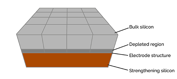
Figure 4: Back Illuminated sensor, before etching.
Now, we can etch away the bulk silicon as shown in Figure 5. This is a physical process. Chemicals are added to the bulk silicon surface and physically polished in a polishing machine. As you polish away, the thickness of this bulk silicon gets thinner and thinner and thinner until it's pretty much all removed or 99% removed. Now the depleted region is exposed, and there is a significant further improvement in quantum efficiency.
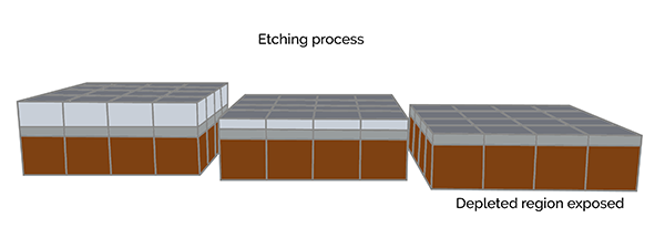
Figure 5: The etching process of a back-illuminated sensor.
At this point is we've removed everything that could possibly be blocking light hitting that sensor, hitting that pixel. Efficiency has gone up quite a bit. It's not perfect, but it's made a big improvement with peak quantum efficiency at ~ 70%. But is that as good as it gets? And why is the quantum efficiency not higher? The answer is due to reflections.
A lot of light that hits that bare metal surface is reflected off. Silicon is quite shiny, but we can deal with this. We can add anti-reflection coatings, these are coatings which minimize reflections and can only be added to a flat surface, so would not work for front-illuminated models. Adding the anti-reflection coating, means more light gets as far as the silicon, and less light is reflected. The result is you get an increase in quantum efficiency.
Anti-reflection coatings are not perfect and need to be tailored for wavelength regions. We offer quite a broad range of different anti-reflection coatings for different applications and different customer needs.
Is there anything we can do more beyond anti-reflection coatings? You'll notice that in some quantum efficiency curves there's a considerable decrease in performance in the infrared. That's because, at this part of the spectrum, light can actually pass right through the depleted region all the way through into the bulk and never be detected.
So, what we can do is we could make this depleted region thicker, then the light would have to pass through more of it and, therefore, increase the possibility of it being detected. So, that's what I've shown here in Figure 6. We've made a very thick depleted region. Now, as the light comes down, there's more chance that it will be turned into a photoelectron.
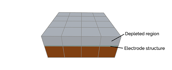
Figure 6: Deep Depletion CCD.
With the further addition of an infrared coating, we can see a huge improvement in performance in the red part of the spectrum. But deep depletion sensors are not perfect, firstly they're an expensive option.
In summary, there are quite a few CCD variants tailored to different applications, different techniques, and, in particular, different budgets.

© Oxford Instruments 2026
