Resources
 Part of the Oxford Instruments Group
Expand
Collapse
 Part of the Oxford Instruments Group
Standard back-illuminated, deep-depletion (BI-DD) CCDs offer quantum efficiencies (QE) up to 95% in the near-infrared (NIR) This makes them the detector of choice for photoluminescence, Raman or plasmonics spectroscopy in the 700 - 1,100 nm range. One disadvantage of deep-depletion devices has been a significant associated increase in dark current (~100 times) compared to standard back-illuminated, visible-optimized CCDs. A new generation of Low Dark-Current, Deep-Depletion (LDC-DD) CCDs now overcomes this limitation, and challenges the need for liquid-nitrogen (LN2)-cooling for photonstarved NIR spectroscopy.
Dark current is a source of noise inherent to CCDs. It arises from thermally generated charges in the silicon lattice over time. Cooling is the most efficient means of reducing dark current in CCD devices, and there are a number of methods (incl. combinations) traditionally used, such as air, liquid coolant, liquid nitrogen (LN2) and thermoelectric (TE). A new generation of back-illuminated, deep-depletion CCDs (LDCDD) now offers excellent dark-current characteristics whilst offering >95% QE in the NIR. This technical note analyses the benefits of this technology by considering the influence of temperature on quantum efficiency (QE) and dark current. It also aims to show that ‘cooler is not necessarily better’, and that the combination of LDC-DD and TE-cooling obsoletes the need for LN2 cooling technology for BI-DD CCDs.
The QE of a CCD is governed by its ability to absorb incoming photons in the photosensitive silicon region. It is only in this region that photons are converted into electron-hole pairs, which are then confined by means of electric fields into a ‘pixel’. The charges held in those pixels can then be transferred and detected.
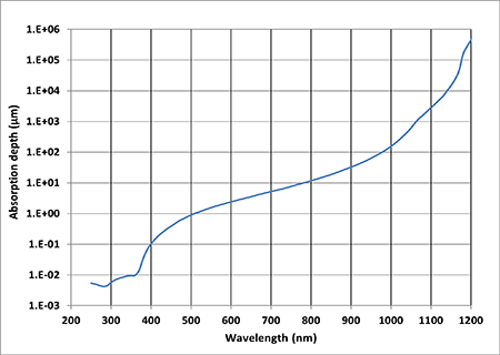
Figure 1: Absorption depth in Silicon at 300K as a function of incident photon wavelength
Shorter wavelength photons (blue light) are absorbed close to the silicon surface, while longer wavelength photons can travel deeper into the silicon matrix before being absorbed. Photons above 1.1 μm do not have enough energy to create a free electron-hole pair that could be detected: a silicon CCD is effectively transparent at these longer wavelengths.
Fig. 1 shows the absorption depth of photons as a function of wavelength in crystalline silicon.
In front-illuminated CCDs, incoming photons must first transverse a polysilicon electrode structure and a silicon oxide (SiO) insulating layer (see Fig. 2). The electrode structure can absorb and reflect part of the incoming photon flux before it reaches the ~ 15 μm thick photosensitive region. This absorption is extremely pronounced in the ultraviolet (< 350 nm), but also limits the peak QE of such devices to around 50% in the visible.

Figure 2: Typical front-illuminated CCD (cross section)
In order to eliminate the losses incurred at the front surface, a backilluminated (BI, Back-thinned) configuration can be adopted. When a device is back-thinned, the bulk substrate is removed by mechanical grinding and chemical etching so that light can enter from the back surface directly into the active photosensitive region. These devices can exhibit peak QE of up to 95% with appropriate anti-reflection (AR) coatings.

Figure 3: Typical back-illuminated CCD (cross section)
NIR QE of standard back-illuminated CCDs can be further enhanced by the use of a thicker photosensitive region (typ. 30-50 μm) and higher resistivity material.
These devices are known as back-Illuminated, deep-depletion (BI-DD) CCDs.
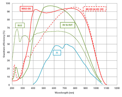
Figure 4: Typical QE performance at +25ºC of front-illuminated (‘FI’), back-illuminated visible-optimized (‘BV’), UV-enhanced silicon back-illuminated (‘BU2’) and back-illuminated deep-depletion CCDs with NIR AR-coating (‘BR-DD’) and broadband dual AR-coating (‘BEX2-DD’). The new BI ‘LDC-DD’ and ‘BR-DD’ have identical QE characteristics.
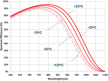
Figure 5: Typical QE variation with cooling temperature of backilluminated, deep-depletion CCD with NIR-optimized AR coating. Data supplied by sensor manufacturer [2]
The absorption depth of photons in the silicon can increase with cooling[1]. This is especially pronounced in the near-infrared, and effectively means that the CCD becomes increasingly transparent to NIR photons. This lower probability of absorbing a NIR photon translates into a decrease in QE (see Fig. 5).
BI-DD CCDs present the best QE in the 750 – 1,100 nm region, up to 95%, but this also means that they are the most prone to QE variation with cooling temperature. This is a consequence of band-gap shifting. At an illustrative wavelength of 950 nm, the probability of an incoming photon generating a detectable photoelectron in the photoative layer of a CCD can drop by up to 50%.
| -20°C | -70°C | -100°C | -120°C | |
| Relative QE drop from +25°C | 16% | 34% | 44% | 50% |
Since a CCD must first collect the incoming photons before detecting the associated photo-electron(s) generated in the active silicon region of the sensor, any decrease in QE must therefore be weighed against the actual dark current improvement benefit for a given experimental scenario.
The following section will focus on the impact of cooling on dark current alone for both standard BI-DD and the new BI LDC-DD technology. The effect on signal-to-noise performance – combining the influence of both QE and dark current variation influence - will be examined subsequently.
In order to better understand the limitation in dark current for current deep depleted devices it is first necessary to understand some concepts regarding CCD structure and how these influence dark current behaviour.
Scientific CCDs are usually manufactured on epitaxial silicon with a thickness of the order of ~15 μm. A typical CCD is made up of pixels which are defined by the permanent channel stops in one direction and by the image phases in the perpendicular direction. (see Fig. 6).
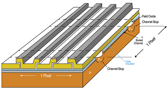
Figure 6: Pixel architecture of a buried channel 3-phase
The image phases are electrode gates that run across the outer surface with the photosensitive region below. Applying a voltage to an electrode gate depletes the region below of electrons producing a potential well often referred to as the ‘depletion region’. It also causes any charge to gather under the nearest most positive (in voltage) phase and by controlling when this voltage is applied, we can define individual pixels and transfer them, on mass, accross the CCD area and into the readout register.
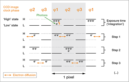
Figure 7: Electron signal shifting in 3-phase ‘NIMO’ CCDs (image area row clocks). Most of the dark current is generated when the image clock (φ1) is held high during CCD exposure (circled). Photoelectron transfer is achieved by ‘toggling’ sequentially the image clocks φ1, φ2, φ3)
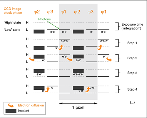
Figure 8: Electron signal shifting in 3-phase ‘IMO’ CCDs (image area row shift). Implants are inserted below one of the image clocks (φ2) to allow setting of image phases voltage low during CCD exposure time and keep dark current under control
At all times at least one of the gate electrodes must be low while the other(s) are high, even during transfer. This is to ensure that charge in one pixel is not mixed with charge from its neighbouring pixels. Electronically this is not a problem to arrange, and is generally referred to as ‘clocking’. This configuration is referred to as Non Inverted Mode Operation (NIMO) (see Fig. 7)
However it turns out that about 100 times more dark current is generated when any image clock is held high compared to low. This can lead to a substantial build-up of dark signal during long integrations.
The origin of this dark current are defects in the interface between the oxide insulating layer and the silicon. These defects are a source of electrons into the conduction band. These electrons are trapped but can be thermally excited, making dark current very temperature dependent.
By keeping the clock level sufficiently low, holes from the channel stops can be attracted into this interface and ‘neutralize’ the electron sources. When this state is reached it is referred to as ‘pinning’..Further lowering of the phase potential will have no effect inside the silicon simply because more holes arrive to pin the voltage, hence the name.
Adding an implant below one of the electrode gates will generate a small voltage step which acts as a barrier between pixels even when all the electrodes are low, i.e. during the integration period. The device can still be clocked successfully, as the large clock amplitudes can easily overcome the smaller implant offset and thus the charge can still be read out (see Fig 8). This technology is referred to as Inverted Mode Operation (IMO) or Multi Phase Pinning (MPP), another version of this which has the same effect is called Asymmetric IMO (AIMO).
Fig. 9 shows the dark current characteristics versus cooling temperature of a standard back-illuminated, deep-depleted CCD (dotted orange line) and the new BI LDC-DD CCD (red line).
At an equivalent pixel size of 15 μm, the LDC-DD shows a significant 10 times dark current performance improvement when compared to a standard deep-depletion CCD.
LDC-DD dark current performance at the lowest cooling temperature is almost identical to standard ‘AIMO’ CCDs.
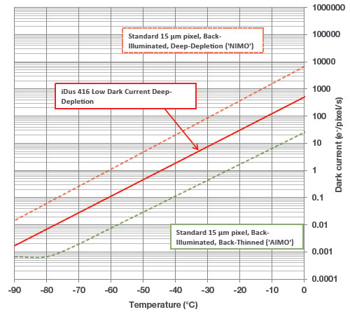
Figure 9: Dark current versus temperature for traditional backilluminated, deep-depletion CCD (dotted orange), standard backilluminated visible-optimized CCD (dotted green) and the new backilluminated LDC-DD CCD (solid red)
The disadvantage of the elevated dark current on standard deep-depleted devices has meant a compromise has to be made: either improved NIR QE response and higher dark current or lower QE response and low dark current.
The reason for this higher dark current has been the inability to ‘pin’ a deep-depleted CCD device. To date neither IMO nor AIMO have been available in conjunction with deep depletion, since inverting (or pinning) the surface during integration reduces the voltage available. This therefore restricts depletion, limiting the advantage of a high resistivity substrate.
However we at Andor have partnered with E2V in order to overcome this restriction, and bring the groundbreaking back-illuminated LDCDD technology to the Academic and Industrial world to greatly facilitate photon-starved spectroscopy acquisition in the NIR. This virtually obsoletes the very inconvenient and unpractical LN2 cooling approach (compared to maintenance-free thermo-electric (TE) cooling).
Signal-to-noise is an essential tool for assessing the combined effect of QE and noise variation in CCDs. It is the achievable signal-tonoise which is of key importance when assessing the performance of any detector in terms of its sensitivity. For CCDs, it can be defined as follow:

Where S is the photon signal, NRN the readout noise, NDN the dark noise, NCIC the spurious charge noise or clocking-induced discharge and NSN the incoming signal shot noise. It can also be expressed as:

Where QE refers to the sensor quantum efficiency (%), I the incoming photon flux (photons/s), t the exposure time (s) and DC the dark current (e-/pix/s or e-/CCD column/s).
Since CCD cooling impacts both dark current and sensor QE, one must consider the following:
The following scenarios look at a SNR performance in the context of spectroscopy, where the signal is vertically binned in a number of rows on the CCD. The impact of the lower dark current of the LDCDD technology on SNR is shown on Fig. 10.
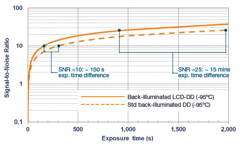
Figure 10: Dark current versus temperature for traditional backilluminated, deep-depletion CCD (dotted orange), standard backilluminated visible-optimized CCD (dotted green) and the new backilluminated LDC-DD CCD (solid red)
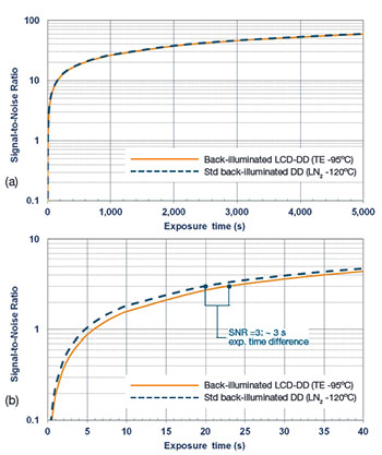
Figure 11: (a) SNR performance of back-illuminated LDC-DD (TEcooled at -95°C) vs standard back-illuminated, deep-depletion (LN2-cooled at -120ºC). Very low photon flux scenario of 1 photon per binned area per second (or 1 photon per 15 μm pixel every 2 minutes) at a wavelength of 850 nm. Binned area is 15 μm wide x 2 mm high (b) Details of the lower CCD exposures region.
Both technologies can achieve good SNR performance. However, the back-illuminated LDC-DD provides equivalent SNR at much shorter CCD exposure times.
In the scenario above, the back-illuminated LDC-DD CCD will achieve a good SNR of 10 with an exposure time of nearly 2 minutes shorter. For a SNR of 25, this difference is ~15 minutes.
Liquid nitrogen-cooled CCDs typically operate at -120°C, and have been considered as the standard for photon-starved NIR spectroscopy applications for decades.
Modern TE-cooled CCDs can achieve -100°C, while offering great advantages:
Fig. 11 shows a very challenging photon regime, and compares the SNR performance of an LN2-cooled BI-DD CCD at -120°C with a back-illuminated LDC-DD CCD TE-cooled to -95ºC.
In this extreme light level scenario, SNR performance between the two technologies is identical for exposure times greater than ~ 30 s). At shorter exposure times, the difference in SNR at a given exposure time is less than 10%, which is minimal.
At higher photon flux, the trend is even more pronounced, with an even closer match at the shortest exposure times.
In conclusion: with the combination of -95°C TE cooling and backilluminated LDC-DD technology, the highest detection performance in the NIR can be achieved even at an extremely challenging photon flux. At higher photon flux, this technology combination will exceed the performance of standard -120°C, LN2-cooled back-illuminated BI-DD CCDs. So when looking for the best NIR sensitivity and the most convenient cooling means, Andor’s iDus 416 -95*deg;C TE-cooled platform with back-illuminated LDC-DD CCD technology has no equivalent.
Optical etaloning is an important point to be mindful of when working with back-illuminated CCDs in the NIR. The back-illuminated LDCDD CCD benefits from a fringe-suppression process implemented during sensor manufacturing, which helps to ‘break’ the Fabry-Pérot étalon formed by the reflections in the CCD depletion region. The maximum peak-to-peak fringing modulation typically varies from 1-5%: these variations are inherent to the manufacturing process at CCD batch level. Refer to Andor technical note “Optical Etaloning in Charge Coupled Devices (CCDs)” [3] for further details on optical fringing in CCDs.
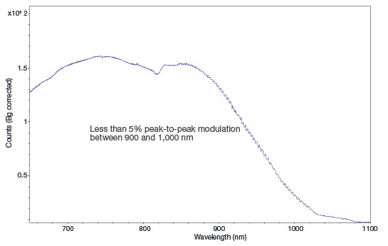
Figure 12: Full Vertically Binned (FVB) spectra of a broadband tungsten source acquired with an iDus 416A-LDC-DD and a Shamrock 750 spectrograph
