Scientific CMOS, or sCMOS, is a breakthrough technology based on next-generation CMOS Image Sensor (CIS) design and fabrication techniques. sCMOS is poised for widespread recognition as a true scientific grade CIS, capable of out-performing most scientific imaging devices on the market today. This is a result of an advanced set of performance features that render it absolutely ideal to high fidelity, quantitative scientific measurement.
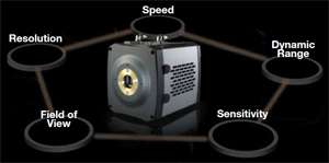
sCMOS technology stands alone in its ability to simultaneously deliver on many key performance parameters, overcoming the 'trade-offs' that are inherent to current scientific imaging technology standards, and eradicating the performance drawbacks that have traditionally been associated with conventional CMOS imagers.
Unlike previous generations of CMOS and CCD-based sensors, sCMOS is uniquely capable of simultaneously offering:
- Extremely low noise
- Rapid frame rates
- Wide dynamic range
- High resolution
- Large field of view
sCMOS – No compromise
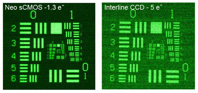
The 5.5 megapixel sensor offers a large field of view and high resolution, without compromising read noise, dynamic range or frame rate. Read noise is exceptional, even when compared to the highest performance ‘slow-scan’ CCDs. The fact that the sCMOS device can achieve down to 1 electron rms read noise while reading out 5.5 megapixels at 30 frames/sec renders it truly extraordinary in the market. Furthermore, the sensor is capable of achieving 100 full frames/sec with a read noise down to 1.3 electrons rms. By way of comparison, the lowest noise Interline CCD, reading out only 1.4 megapixels at ~ 16 frames/sec would do so with ~ 10 electrons read noise.
The low noise readout is complemented by up to 30,000:1 dynamic range. Usually, for CCDs or EMCCDs to reach their highest dynamic range values, there needs to be a significant compromise in readout speed, yet sCMOS can achieve this value while delivering high frame rates. The unique dual amplifier architecture of sCMOS allows for high dynamic range by offering a large well depth, despite the relatively small 6.5 μm pixel size, alongside lowest noise. A 1.4 megapixel Interline CCD with similarly small pixels achieves only ~1,800:1 dynamic range at 16 frames/sec.
| Parameter |
sCMOS (Zyla) |
Interline CCD |
EMCCD |
| Sensor Format |
5.5 megapixel |
1.4 to 4 megapixel |
0.25 to 1 megapixel |
| Pixel Size |
6.5 μm |
6.45 to 7.4 μm |
8 to 16 μm |
| Read Noise |
1.2e- @ 30 frames/sec
1.45e- @ 100 frames/sec |
4 - 10 e- |
< 1 e- (with EM gain) |
| Full Frame Rate (max.) |
100 frames/sec @ full resolution |
3 to 16 frames/sec |
~ 30 frames/sec |
| Quantum Efficiency (max.) |
57% |
60% |
90% 'back-illuminated'
65% virtual phase
|
| Dynamic Range |
25,000:1
(@ 30 frames/sec) |
~ 3,000:1
(@ 11 frames/sec) |
8,500:1
(@ 30 frames/sec with low EM gain)
|
| Multiplicative Noise |
None |
None |
1.41x with EM gain
(effectively halves the QE)
|
Scientific CMOS (sCMOS) Architecture
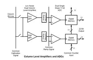
The sensor features a split readout scheme in which the top and bottom halves of the sensor are read out independently. Each column within each half of the sensor is equipped with dual column level amplifiers and dual analog-to- digital converters (ADC), represented as a block diagram in below. This architecture was designed to minimize read noise and maximize dynamic range simultaneously.
The dual column level amplifier/ADC pairs have independent gain settings, and the final image is reconstructed by combining pixel readings from both the high gain and low gain readout channels to achieve a wide intra-scene dynamic range from such a small pixel pitch.
Each pinned-photodiode pixel has 5 transistors (‘5T’ design), enabling the novel ‘global shutter’ mode (described in more detail below) and also facilitating correlated double sampling (CDS) and a lateral anti-blooming drain. The sensor is integrated with a microlens array that serves to focus much of the incident light per pixel away from the transistors and onto the exposed silicon, enhancing the QE (analogous to use of microlenses in interline CCDs to focus light away from the column masks).
The sensor is configured to offer low dark current and extremely low read noise with true CDS.The sensor also has anti-blooming of >10,000:1, meaning that the pixels can be significantly oversaturated without charge spilling into neighboring pixels. It is also possible to use the anti-blooming capability to hold all or parts of the sensor in a state of ‘reset’, even while light is falling on these pixels. The time to transfer charge after the exposure is complete is less than 1μs, rendering the sensor useful for fast electronic shuttering and ‘double exposure’ techniques such as Particle Imaging Velocimetry (PIV).

