Resources
 Part of the Oxford Instruments Group
Expand
Collapse
Part of the Oxford Instruments Group
Application Notes
Author: Thomas Woodward, Adam Wise, Shayne Harrel, Jenny Goulden & Antoine Varagnat
Published: 01 Nov 2022 · Last updated: 23 Mar 2023
The advent of rapid, cost-effective, high-powered lasers are driving forward advancements in the fields of for soft X-ray and EUV imaging, ptychography, spectroscopy and tomography. This coupled with increasing investment in industrial EUV lithography & semiconductor metrology processes is creating demand for fast, high resolution and sensitive detectors in the 20 eV to 10 keV range.
Here we present the latest detector developments in the field of sCMOS for direct EUV and soft X-ray detection. We demonstrate how sCMOS technology is able to overcome the limitations of slow scan CCD technology to provide high resolution direct EUV and soft X-ray detection with a greater than 16-fold speed increase whilst maintaining low noise compared to classical CCD detectors.
The industrial and scientific landscape of the modern world is rapidly evolving, and multiple factors are now coming together to push instrumentation manufacturers towards the next generation in ultra-sensitive, fast, low noise instrumentation. Increasingly large industrial investment in EUV lithographic semi-conductor manufacturing processes is driving the need for fast, sensitive and high throughput imaging solutions for applications such as lithographic mask inspection & wafer inspection to continue advancing Moore's Law forward and enabling the creation of cost-effective sub nanometre transistors.
Furthermore, within research markets, investment in large scale research infrastructure projects such as the extreme light infrastructure (ELI) project are driving affordable high powered laser solutions into the laboratory research market enabling unprecedented access for many researchers to high power, high repetition rate light sources for the high harmonic generation for soft X-ray and EUV pulses. Additionally, synchrotrons across the world are upgrading their light sources to fourth generation designs offering orders of magnitude improvements in brightness and beam coherence1.
Combined, all these factors are creating demand for fast, high resolution and sensitive detectors in the 20 eV to 10 keV range. To date one of the main methods of capturing EUV/soft X-ray photons for applications such as semiconductor metrology, X-ray absorption spectroscopy, soft X-ray microscopy & tomography has been the use of 2D slow scan CCD detectors. In this paper we discuss the technological bottlenecks that exist in 2D detector technologies for direct EUV and soft X-ray detection and, in particular, between CCD and sCMOS technology. We also discuss what is required to make sCMOS technology viable for direct EUV & soft X-ray detection, the steps taken to achieve this, the current state of the art, existing applications already using this technology and future outlooks for the development of this technology as a viable solution to meet the challenging needs of industrial and research EUV/soft X-ray application market.
2D detectors utilise the photoelectric effect - the generation of electron hole pairs upon the absorption of electromagnetic radiation - to convert incident visible photons or X-rays into photoelectrons that can then be accumulated and read out within a 2D detector2. Two key 2D detector technologies are used for direct X-ray and EUV imaging: Charge coupled devices (CCDs) and more recently scientific complementary metal oxide semiconductors (sCMOS) as shown in Figure 1.
CCDs detectors are integrated circuits etched into a silicon surface to define light sensitive elements into a pixel array. Photons striking the surface of a CCD are converted into photoelectrons, the charge generated is collected and transferred from individual pixels into a readout register where it is then converted from an analogue to digital signal at a readout node and the various output intensities brought together to construct an image.
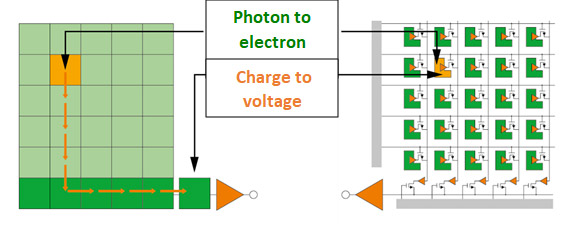
Figure 1: A diagram showing the pixel layout and design of a CCD sensor (left) and sCMOS sensor (right)
CCD detectors have long been the go-to technology for direct X-ray/EUV imaging as they offer high resolution, deep well depths, low noise readout at slow speeds and consequently relatively good dynamic range. Furthermore, CCDs have several unique features that make them well suited for ultra-sensitive scientific imaging: CCDs can be deep cooled to temperatures of <-100o minimizing thermally generated electrons (dark current) which reduces the overall noise of the sensors during long exposures. Additionally, CCDs are available in relatively large pixel sizes >15 µm, which is advantageous for reducing charge splitting events in X-ray/EUV detection. Lastly CCDs are available with deep depleted sensors enabling the detection of higher energy X-rays up to 20 keV (Figure 2).
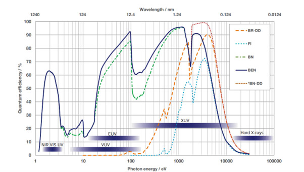
Figure 2: Soft X-ray sensor quantum efficiencies for varying depletion layer thickness and sensor illumination geometries in CCD sensors
However, CCD technology has a few key drawbacks that have put it at odds with the increasing drive towards higher imaging and spectroscopy readout rates demanded by the research community. CCDs have a limited number of readout nodes (normally up to four readout nodes) available, which limits their maximum readout speed. Furthermore, the faster a CCD is readout the greater the readout noise and the higher the signal required to overcome the read noise floor in an image, this also limits the dynamic range a fast CCD can achieve. Lastly, CCDs require a mechanical shutter to avoid signal gradients across the sensor surface which is still vulnerable to light while an image is being readout, this can lead to increased downtime and maintenance costs in the long term as mechanical shutters are prone to failures after high numbers of cycles - a consequence more likely in rapid imaging applications such as tomography and ptychography.
Scientific CMOS or sCMOS is an ultra-sensitive low noise, fast high-dynamic range advancement of CMOS detectors which classically were relatively high read noise devices. Prior to the development of sCMOS technology in 2009 in a consortium between Andor Technology - Oxford Instruments3, PCO and Fairchild (later BAE), scientists were limited to using either CCD or EMCCD cameras for quantifiable scientific measurements. sCMOS detectors effectively miniaturise the readout electronics of a CCD array such that each individual pixel has its own array of electronics to convert charge to voltage4.
sCMOS devices utilise a 4-5T (T=Transistors) in pixel amplifier design which gives a greatly improved read noise relative to CMOS sensors (typically 2-3T). The development of sCMOS enables whole rows of pixels to be read out simultaneously resulting in the ability to achieve rapid frame rates and enables global and rolling shutter configurations whilst maintaining low read noise, high sensitivity, and dynamic range.
sCMOS sensors have high resolution, and a large array of pixel sizes available similar to CCDs. However, sCMOS technology inherently has several unique advantages over CCD devices: first and foremost, sCMOS devices can read out exceptionally fast but combine this with very low read noise regardless of the readout speed. This means it is possible to readout rapidly and maintain a high number of greyscales/dynamic range within an image. Secondly, sCMOS detectors do not require a mechanical shutter, making them more reliable and lower maintenance in the long-term relative to CCDs.
sCMOS devices have been rapidly adopted into the life science microscopy community and a variety of applications in the physical sciences such as quantum, fast spectroscopy, combustion, and plasma imaging also use sCMOS cameras. However, until recently CCDs were the primary choice for the direct soft X-ray and EUV imaging and spectroscopy marketplace. sCMOS was not used in the EUV/soft X-ray marketplace and to understand this we must first think about what makes a detector suitable for the imaging of X-rays/EUV photons.
There are three key parameters that determine how well a sensor will detect X-ray/EUV photons. Firstly, the material a detector is constructed from determines the sensor’s probability to absorb a given X-ray/EUV photon at a given depth. Commonly silicon is used in soft X-ray detection devices as it is good at absorbing relatively low energy X-rays and EUV photons. Other materials such as mercury cadmium telluride are often used to detect harder more energetic X-rays in other direct X-ray detection devices such as hybrid pixel detectors.
Secondly, the thickness of the semiconducting material such as doped silicone in a sensor is critical regarding its ability to absorb X-rays and resist damage. In a semiconducting device the epitaxial layer thickness or active layer denotes the region of the material that is active in absorbing incoming photons and translating them into photoelectrons. The thicker the epitaxial region the higher the probability an incident X-ray photon will be converted into photoelectrons. Additionally, X-rays introduce damage into sensors over time and the thicker the epitaxial layer is the greater a sensors resistance to X-ray damage. However, there is a trade off in that the thicker the epitaxial layer of a sensor, the harder it is to capture the generated photoelectrons within an electric field. Hence, manufacturers of X-ray detectors often must strike a balance between pixel thickness and modular transfer function (the ability of an individual pixel to capture photoelectrons that land in it).
Thirdly, all silicon-based semiconductors sensors have a protective layer or coating on their surface, this is applied to protect the sensor surface from oxidation and damage. Often in visible light applications coatings are applied to help improve quantum efficiency and prevent etaloning. Where sensors are detecting X-rays/EUV photons, coatings, undesirably, act as a barrier that absorb low energy incoming X-ray/EUV photons and reduce quantum efficiency. Hence, especially for low energy X-ray/EUV application a thin coating is critical for good detection performance.
Until recently CCDs have long been the go-to technology for direct EUV and soft X-ray detection, this was primarily driven by the lack of ability to create sCMOS sensors that combined the above requirements of thin coatings and thick epitaxial layers. However, recently the sensor manufacturer Gpixel Inc has produced the first of the next generation of sCMOS sensors for direct EUV/soft X-ray. These first sCMOS sensors for direct X-ray and EUV detection are back thinned, with a minimal passivation later of only 5nm to promote a low energy EUV/soft X-ray response and this, combined with a 9.5 µm epitaxial layer thickness (typical sCMOS is ~3 µm), helps to promote durability and quantum efficiency in the soft X-ray regime. The recorded quantum efficiency in work carried out by Harada et al5 has shown that these sensors demonstrate a better response than comparable CCDs in the 60eV-1keV energy range (Figure 3).
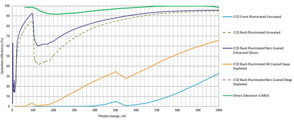
Figure 3: Quantum efficiency comparison between common CCD sensors and the Gpixel EUV/Soft X-ray sCMOS sensor between 60 eV-1keV
This revolutionary development in the detector marketplace is already being used to create direct X-ray and EUV detection cameras that far surpass their equivalent CCD counterparts in terms of speed, sensitivity and dynamic range with cameras now available on the market that can achieve speeds up to 16x faster than a comparable CCD camera (Figure 4).
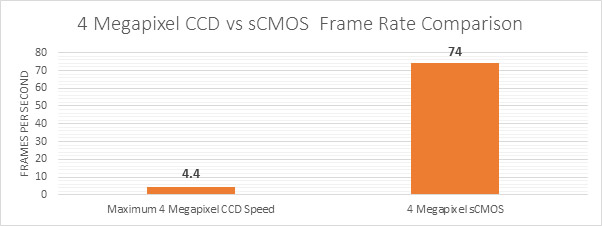
Figure 4: Speed comparison of a 4 Megapixel CCD camera with a 4 Megapixel sCMOS camera
The advent of direct detection sCMOS has implications already for high speed applications such as water window tomography, soft X-ray spectroscopy and ptychography applications. Direct detection sCMOS cameras are already being used for applications such as fast spectroscopy at the EAST tokamak in China, X-ray lens calibration imaging for space telescopes at NASA and EUV & soft X-ray imaging at the Pohang Accelerator Laboratory in South Korea.
Though fast sCMOS for direct X-ray/EUV detection has many advantages relative to slow scan CCDs, it is not without limitations. Currently direct detection sCMOS has very limited quantum efficiency beyond 1 keV and is relatively susceptible to damage over time at higher energies as shown by Harada et al. This is due to the relatively limited epitaxial layer thickness (9.5 µm) of the current generation of Gsense BSI compared to some direct X-ray detection CCD sensors (<50 µm). Hence, CCDs are still the imaging option of choice for >2-3 keV X-ray imaging applications.
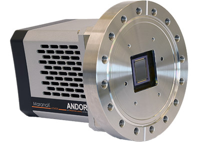
Figure 5: Andor Marana-X Direct X-ray Detection sCMOS Camera6
Currently, the best available field of view available via direct detection sCMOS is currently limited to the 22.5 x 22.5 mm in the Marana-X 4.2 megapixel 11 µm pixel camera (Figure 5) recently launched by Andor Technology. Hence, currently CCDs are still better suited to larger field of view applications with sensor sizes of greater than 61mm x 61mm available.
So, what does the future hold for direct detection sCMOS cameras for EUV/soft X-ray detection? Now the state of the art has advanced such that processes are now available in the fabrication of sCMOS sensors with thicker epitaxial layers and thin coatings it is entirely possible we could see, in the coming years, a large variety of sensors suited for EUV and soft X-ray applications. New sensors can now be generated in a variety of formats such as higher speed, larger areas, smaller or larger pixel formats. Significant challenges, still surround achieving even deeper depleted sCMOS sensors, due to the difficulties in manufacturing higher voltage sCMOS sensors, capable of capturing photoelectrons from pixels at greater epitaxial depths.
CCDs have long been the go-to technology for direct EUV and X-ray imaging & some scattering applications. sCMOS technology is finally being introduced to enable faster, lower noise solutions to meet the market needs of semi-conductor manufacturing, brighter and faster laser sources, and the next generation synchrotron upgrades across the world. sCMOS technology will enable researchers to make the most of brighter, faster, and more intense sources, by supplying detectors with the necessary frame rates to meet the demanding needs of researchers in the coming years. However, CCDs will for the time being retain their place as the go to cameras for imaging and spectroscopy of X-rays in the 3-20 keV energy range for the immediate future.
[1] Winick, H., “Fourth Generation Light Sources,” Proc. Particle Accelerator Conf, (1997) 1.
[2] Janesick, J. R., [Fundamentals of Scientific Charge-coupled Devices], SPIE Press, Washington, 167-268 (2001).
[3] Coates, C., Fowler, B., and Holst, G., “sCMOS, Scientific CMOS Technology, A High-Performance Imaging Breakthrough,” Andor White Paper, www.scmos.com/downloads/ (2009).
[4] Bigasa, M., Cabrujaa, E., Salvib, J., “Review of CMOS image sensors”, Microelectronics Journal, 37, 433-451 (2006).
[5] Harada, T., Teraishi, N., Watanabe, T., Zhou, Q., Bogaerts, J., and Wang, Xinyang., “High-exposure-durability, high quantum-efficiency (>90%) backside-illuminated soft-X-ray CMOS sensor”, App Phys Express, 13, 015502 (2020).
[6] Andor Technology, “Marana-X Specification Sheet”. Specifications Sheet. 2021.

© Oxford Instruments 2026
