Resources
 Part of the Oxford Instruments Group
Expand
Collapse
Part of the Oxford Instruments Group
Application Notes
Author: Andrew P. Carpenter, Adam Wise
Published: 01 Feb 2026 · Last updated: 27 May 2026
High-sensitivity ultraviolet (UV) imaging and spectroscopy are essential for emerging applications such as optical characterization of high-bandgap semiconductors, photolithographic mask inspection, extreme UV (EUV) light source diagnostics, UV Raman spectroscopy for chemical analysis, and plasma dynamics imaging for fusion research. These fields demand detectors with exceptional quantum efficiency (QE), low noise, and high temporal resolution in the EUV–UVC range (10–400 nm). This study employs a comprehensive approach, integrating experimental measurements and simulated data to evaluate the performance of various UV-sensitive EMCCD, CCD, and sCMOS architectures across a range of cutting-edge applications.
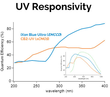
QE curves of UV optimized EMCCD (blue) and sCMOS (orange). Expanded QE curves in inset with visible optimized CCD curve (green).
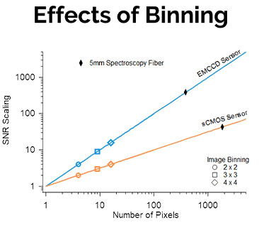
SNR Scaling as a function of the number of binned pixels. Common imaging bins (2x2, 3x3, 4x4) and representative spectroscopy bin (5 mm) are highlighted.
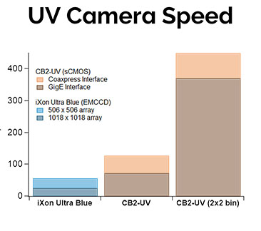
Representative, full-frame, frame rates for UV optimized EMCCD (blue) and sCMOS (orange) sensors.
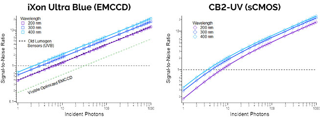 UV optimized EMCCD (left) and sCMOS (right) camera sensitivity calculated at 200 nm (purple), 300 nm (dark blue), and 400 nm (light blue) for a 10 ms exposure time, maximum cooling, and highest bit-depth digitization.
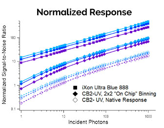 Normalization of pixel size enables performance comparisons within a common optical system (i.e lens arrangement).
Emissions from industrial sites, vehicles, and electricity heat production sites, to name a few, may not always be detectable in visible wavelength bands. For example, the emission of SO2 from crude oil combustion can be detected in the UV when it is otherwise invisible to the naked eye or machine vision cameras.1
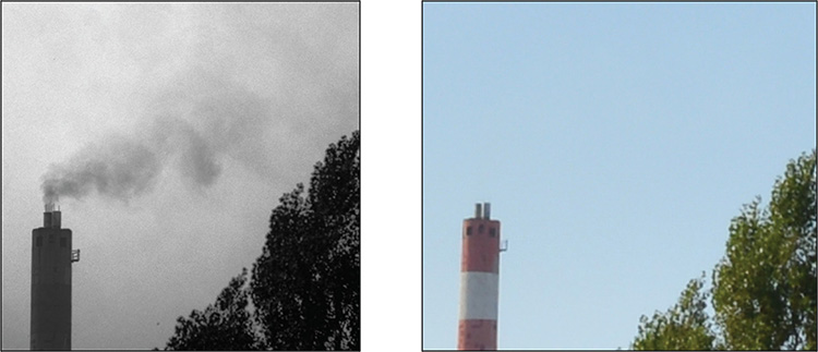
With a f/2.8 100 mm objective the CB2-UV sCMOS was used to detect SO2 from an industrial chimney (left) while the emissions go unnoticed when imaged using a visible wavelength camera (right).
As EUV light sources continue to be developed, UV light sources remain a common fixture in semiconductor photolithography and metrology systems (ex. 193 nm). UV optimized sCMOS and EMCCD cameras are powerful tools to sample small features at and extend the “effective dynamic range” through fast image acquisition.
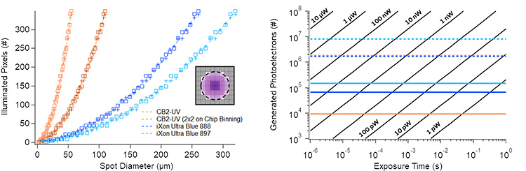
Number of illuminated pixels for a given beam diameter (left) and the saturation level for different exposure times and 193 nm laser fluences (right). Presented for the CB2-UV (orange) and iXon Blue (blue).
Resulting from their pixel level readout architecture, UV optimized sCMOS cameras show great promise to reduce artifacts (e.x. smearing, blooming) and enable high fidelity microspectroscopy experiments.
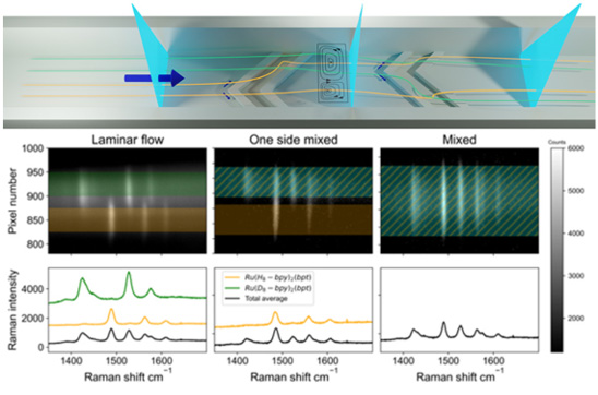
Concept is presented (right) for visible Raman microspectroscopy experiments of a highly dynamic microfluidic mixing system.2 Such a system can be adapted to UV Raman studying biological complexes, material analysis, and for identifying explosives and chemical agents.
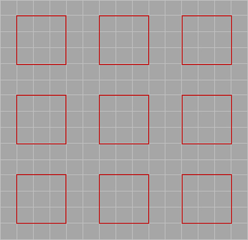
Adaptive Optics (AO) systems are used to correct for atmospheric distortions to incoming wavefronts. Some AO systems rely on laser guide stars with wavelengths outside the wavelength window of the primary observation camera. The third and fourth harmonics of Nd:YAG lasers (355 nm and 266 nm, respectively) are perfectly tuned with the CB2-UV’s QE curve. The multi-windowing function (illustrated right) and 2 x 2 on-chip binning further optimize the sensor for flexible readout operation for Shack-Hartman wave front sensing. With CoaXPress data interference, low latencies also optimize this camera's function for AO applications.
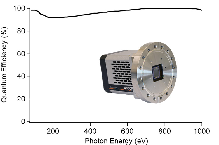
Similar in the VUV and DUV regions, recent innovations in EUV sCMOS technology are delivering unprecedented opportunities for semiconductor and fusion research. As the semiconductor industry moves towards using 13.5 nm (~92 ev) and high NA lasers EUV sCMOS cameras offer unprecedented sensitivity and speed for high throughput applications. In the fusion space EUV technology enables rapid detection of impurities in fusion plasma.
UV optimized sCMOS and EMCCD cameras are well positioned to advance sensitive, low noise, imaging and spectroscopy systems requiring UV detection. From the semiconductor industry to general spectroscopy to on-sky observations, UV imaging and spectroscopy solutions can be optimized to meet experimental needs.
REFERENCES

© Oxford Instruments 2026
