Resources
 Part of the Oxford Instruments Group
Expand
Collapse
 Part of the Oxford Instruments Group
The group ‘Technology of extreme ultraviolet radiation’ at Chair Technology of Optical Systems (TOS), the RWTH Aachen, Germany, investigates applications for laboratory-based XUV gas-discharge sources [1]. Extreme ultraviolet radiation (XUV, 1-50 nm, or EUV at 13.5 nm) enables new optical, analytical and manufacturing technologies because of its characteristic interaction with matter, its short wavelength, and recent progress on light sources and optical components. XUV tools are already deployed by the semiconductor industry in the next generation lithography, which significantly accelerates a further development of XUV technology. Future applications that will support the scientific progress in a variety of fields, such as nanoelectronics or bio-technology, are the scope of their research. Activities include structuring on a nanometer scale using interference lithography, XUV microscopy for imaging of dynamic processes or at-wavelength inspection of multilayer mask-blanks for hidden defects, and characterization of thin film coated surfaces using grazing-incidence reflectometry [2-6].
For the detection of the XUV radiation charge coupled devices (CCDs) with sufficient quantum efficiency at the XUV wavelengths and with low level of noise are needed. Therefore several Andor CCD cameras are used in the group’s laboratories.
XUV Reflectometer
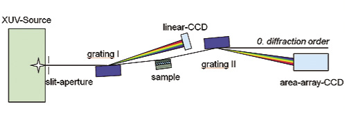
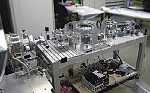
The reflectometry set into the Andor DX440-BN CCD is successfully integrated. The developed XUV reflectometer, shown in Fig. 1 and Fig. 2, consists of two spectrometers.

Fig. 1: Schematic of the grazing incidence XUV reflectometer (GIXUVR)

Fig. 2: Photo of the GIXUVR at the RWTH Aachen

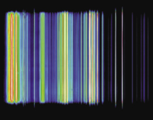
Fig. 3: Line spectrum of the emission of a gas-discharge XUV source measured by the Andor DX440-BN CCD camera
The first spectrometer utilizes a compact backthinned line sensor with the purpose of determining the source emission spectrum.After interaction of the zeroth order of the emission with the sample, the spectrum is analyzed again with the Andor CCD at the end of the beamline. A typical measured line spectrum is shown in the Fig. 3. The DX440-BN also offers the possibility of in-vacuum operation that allow the researchers to perform additional measurements of the scattered radiation.
The pixel size of 13.5 x 13.5 μm² provides a state-of-the- art resolution at this wavelength range. With a sensor size of 2048 x 512 pixels the CCD allows for excellent spectral resolution, as well as a capability to average the signal over 512 lines, thus improving the accuracy of measurements. In comparison to line sensors, which were also investigated, the CCD offers the possibility of a vertical adjustment [7].
XUV Quantum Efficiency
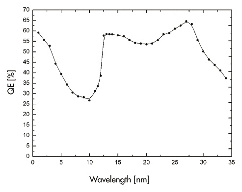
Series of experiments were performed with the Physikalisch Technische Bundesanstalt (PTB) at the synchrotron BESSY in Berlin, Germany, to determine the quantum efficiency at the XUV wavelengths. The quantum efficiency of the Andor DX440-BN CCD in the range from 1 nm to 34 nm is shown in Fig. 4.
The maximum of the QE is at 27 nm wavelength with the value of 64.6%. Due to strong absorption of XUV radiation at the L-absorption edge of silicon a local minimum of 26.8% is situated next to 12.4 nm [8].
In summary, the research group found the Andor DX440-BN detector offers good quantum efficiency in the XUV regime and

Fig. 4: Determined quantum efficiency of the Andor DX440-BN CCD detector from 1 nm to 34 nm wavelength
With thanks to:
Dipl.-Ing. (FH) Sascha Brose
Chair for the Technology of Optical Systems
RWTH Aachen University, Germany
[1] K. Bergmann, S.V. Danylyuk, L. Juschkin, ‘Optimization of a gas discharge plasma source for extreme ultraviolet interference lithography at a wavelength of 11 nm’, J. Appl.Phys. 106, 073309–073309-5 (2009)
[2] S. Danylyuk, L. Juschkin, S. Brose, K. Bergmann, P. Loosen, J. Moers, S. Trellenkamp, G. Panaitov, K. Wambach and D. Grützmacher, ‘XUV interference lithography for sub-10 nm patterning’, Jülich-Aachen Research Alliance - annual report 2008, pp. 49–50 (2009)
[3] L. Juschkin, R. Freiberger, K. Bergmann, ‘EUV microscopy for defect inspection by dark-field mapping and zone plate zooming’, Journal of Physics: CS 186, 012030–012030-3 (2009)
[4] S. Herbert, A. Maryasov, L. Juschkin, R. Lebert, K. Bergmann, ‘Defect inspection with an EUV microscope’, in ‘26th European Mask and Lithography Conference’ edited by U. F. W. Behringer and W. Maurer, Proc. SPIE 7545, 75450O–75450O-9 (2010)
[5] M. Banyay, L. Juschkin, ‘Table-top reflectometer in the extreme ultraviolet for surface sensitive analysis’, Applied Physics Letters 94 (6), id. 063507 (2009)
[6] M. Banyay, L. Juschkin, ‘Spectral sharpening algorithm for a polychromatic reflectometer in the extreme ultraviolet’, Applied Spectroscopy 64 (4), 401–408 (2010)
[7] M. Banyay, S. Brose, L. Juschkin, ‘Line image sensors for spectroscopic applications in the extreme ultraviolet’, Meas. Sci.Technol. 20, 105201–105201-5 (2009)
[8] S. Brose, ‘Experimentelle Untersuchungen zur Adaption von Zeilendetektoren für Anwendungen extreme ultravioletter Strahlung’, diploma thesis, FH Aachen, Jülich (2008)
