Resources
 Part of the Oxford Instruments Group
Expand
Collapse
 Part of the Oxford Instruments Group
Given the high level of bond saturation, the electronic and optical behavior of dielectric oxides is largely governed by defects in their lattice. The relevance of oxygen vacancies and impurity atoms, especially on the material’s optical response, is reflected even in their name as ‘colour centres’. For a long time, only the non-local and averaging optical signature of colour centres could be probed, as the attainable spatial resolution of optical spectroscopy was well below the mutual distance between them. As different defects locate in different chemical environments, the respective spectral fingerprints consequently suffered from large inhomogeneous broadening effects. With the advent of scanning probe techniques as a means to spectroscopically address individual atomic sites, and with the availability of powerful optical detectors capable of single photon sensing, luminescence spectroscopy of isolated colour centres has become possible nowadays [1].
The experiments were performed in a liquid-nitrogen cooled scanning tunneling microscope (STM), with the microscope head being positioned inside a parabolic mirror to collect photon emission from the tip-sample junction. A second, off-axis mirror above the microscope reflects the light out of the vacuum chamber into the entrance slit of a CCD detector (Andor iDus DU420A-BEX2-DD) attached to a spectrograph (Andor Kymera-193i-A). Individual colour centres can now be identified by scanning the dielectric surface with atomic resolution. To probe their luminescence, the tip is positioned above the defect of interest and energy-selected electrons are injected into the site for a given time. Luminescence spectra with good signal-to-noise ratio can be acquired by collecting the outgoing photons for 180 s at 1 nA current.
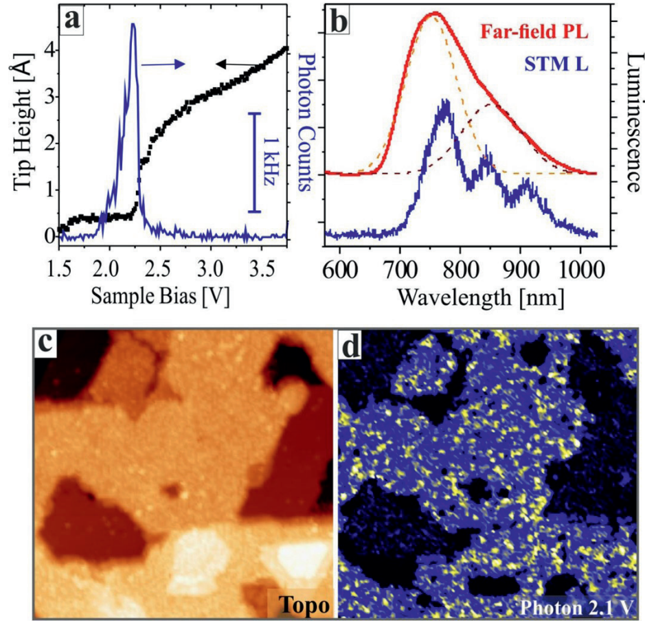
The experiments discussed here were performed on a Cu2O thin film grown on an Au(111) single crystal. With a direct, forbidden band gap of 2.15 eV, cuprous oxide is of large interest for photovoltaic and photocatalytic applications. Its optical properties are governed by a series of para- and orthoexcitons, as well as by several defect-mediated decay channels in the lattice. The far-field photoluminescence of the oxide film is determined by exciton recombination via single and double charged O vacancies (colour centers), resulting in two broad emission bands centered at 750 and 850 nm (Fig. 1). To probe the local luminescence, electrons with 2.2 eV energy above the Fermi level were injected into individual color centres. At this energy position, an O defect state is reached inside the oxide band gap, serving as the initial state for radiative decays into hole states at the valence-band top. The excitation channel shows high selectivity and already a small deviation of the electron energy from the resonance position leads to a drastic decay of the emitted intensity (Fig. 1a). The spectral characteristic of the luminescence is controlled by plasmonic excitations in the tip-sample cavity of the STM and contains no direct information on the actual colour centre. It typically displays a sequence of emission maxima between 700 to 950 nm, coinciding with the window of plasmonic field enhancement in the Au-Au tunneling contact (Fig. 1b). Even though no spectral information is obtained on oxide colour centres, their spatial localization in the oxide surface can be probed with sub-nanometer resolution with our experimental approach. For this purpose, the tip is scanned over a selected Cu2O region and the emission response along the trajectory is detected with an ultra-sensitive photomultiplier. So recorded photon maps display a disordered arrangement of highly localized emission centres, each one representing a single oxygen vacancy in the Cu2O surface (Fig. 1c,d). Our measurements demonstrate how the density of oxygen defects can be tailored via the oxygen chemical potential during Cu2O preparation. To achieve also spectral insights into the luminescence of individual colour centres, the plasmonic response of the STM cavity needs to be suppressed, e.g., by using non-plasmonic materials for both, tip and sample. Respective measurements are currently performed in our labs.

Figure 1. (a): STM emission yield and tip-height signal measured in a constant-current ramp from 3.75 to 1.5 V (I = 1 nA). The sharp intensity maximum marks the condition for resonant tunneling into O defect states in the Cu2O band gap. (b): Far field PL and STM luminescence spectra of a 10 nm Cu2O/Au(111) film. Whereas radiative electron decay via oxygen vacancies controls the emission response in the former case, plasmonic excitations in the STM cavity are responsible in the latter one. (I = 1nA, 180 s accumulation, 100 K). (c) To-pography and (d) corresponding photon map of a Cu2O/Au(111) film taken at 2.1 V sample bias (80 × 80 nm2, I = 1 nA). Each emission spot corresponds to a single colour centre in the oxide surface.
References
A. Gloystein et al., J. Phys. Chem. Lett. 14 (2023) 17.
Contact:
Prof. Dr. Niklas Nilius Carl-von-Ossietzky
University Institute of Physics, D-26111 Oldenburg Germany
E-mail: niklas.nilius@uni-oldenburg.de
Phone +49-441-798-3152
https://uol.de/en/raspe
Date: June 2023
Author: A. Gloystein, J. Gorobez, N. Nilius
Category: Application Note
