Ultrafast transmission electron microscopy is a promising technique for the observation of charges moving on their natural femtosecond time-scale and nanometer length-scale [1,2].
Approaches to time-resolved electron imaging, in which the dynamical response of a sample to a pulsed excitation is followed by a time-delayed electron probe, are usually based on the emission of short electron pulses from photocathode triggered by a few-femtosecond laser pulse. Sharply etched metal tapers have been demonstrated to be especially well-suited electron emitters for ultrafast electron imaging. Such a geometry supports a localized surface plasmon at the very apex of the emitter in conjunction with high electric field strengths, resulting in the localized electron emission from a few-nanometer cathode region.
Here we describe a field ion microscope (FIM) [3], which was realized in order to characterize sharply etched metal tapers prior to their implementation in ultrafast transmission electron microscopy. We aim for a more reliable tip production process and in situ testing of novel electron sources with regard to their coherence properties and suitability as ultrashort electron pulse emitters.
Setup and Working Principle
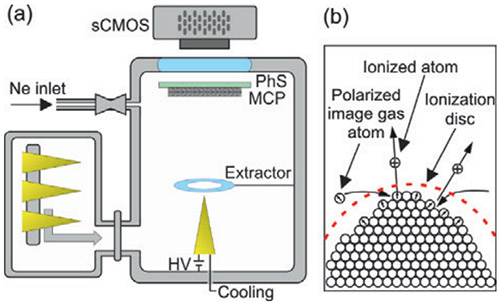
Figure 1. (a) Schematic drawing and (b) working principle of the field ion microscope for inspection of electron emitter tips.
The sharply etched nanotapers are mounted inside a vacuum system consisting of a load-lock and main chamber (Figure 1a). Both are evacuated by turbo pumps, with the pressure in the gate chamber reaching 2.10-8 mbar and 5.10-10 mbar in the main chamber, respectively. A gas inlet allows for a well-controlled injection of Neon as an image gas, typically at a partial pressure of about 4.10-5 mbar. Up to four tapers can be stored in the load-lock chamber. Using a transfer arm, one taper can be picked and placed into the main chamber, where it is mounted in an adjustable sample holder. A voltage of up to +15 kV is applied to the tip with respect to the chamber at ground potential. Using a closed-cycle cryostat, the taper is cooled to temperatures down to 20 K. A circular extractor electrode at ground potential is placed in front of the taper. At a variable distance (typically 10 cm), a sensitive ion detector is mounted, consisting of a two-stage micro channel plate (MCP) stack and a phosphor screen. The angular alignment of the taper axis relative to the detector can be adjusted by 2-axis rotational feedthrough connected to the sample holder. The ion image formed on the phosphor screen is recorded through a window using an sCMOS camera (Andor Neo-5.5-CL3).
For the generation process of noble gas ions at the tip apex, we consider their interaction with the strongly enhanced static electric field within this region. In a first step, neutral Neon atoms are electrically polarized in the apex field, resulting in their preferentially absorption at the apex. Typical apex field exceed 1 V/nm enabling tunneling ionization of atoms at a close distance to the surface of the apex (ionization disc, see Fig. 1b). The positively charged ions are accelerated towards the ring-shaped extractor electrode, beyond which they drift through a field-free range towards the MCP. The image that forms on the phosphor screen represents a local map of the electric field strength at the emitter apex, which is enhanced at crystallographic surface steps and defects.
Tip Production and Characterization
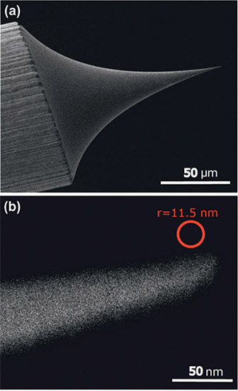
Figure 2. Scanning electron microscopy images of the tip examined in the field ion microscope.
The tips used here are electrochemically etched from polycrystalline Tungsten wires with a 125 μm diameter [4]. A voltage of 12 V is applied between a beaker with a sodium hydrate solution and a sodium hydrate membrane that stretches across a ring electrode placed about 0.5 mm above the surface of the solution. The Tungsten wire is held at the top such that it pierces the membrane and its end is immersed in the solution in the beaker. This closes the electric circuit and as the voltage is applied, the etching process is started in the lamella-immersed part of the wire. A meniscus forms where the solution is in contact with the wire, which leads to the typical shape of the etched tapers (see Fig. 2a).
The etching process is stopped automatically as the lower part of the wire is severed and the circuit is disrupted. Figure 2 shows scanning electron microscopy images of one of the Tungsten tips produced by this procedure. It has a rather narrow opening angle of < 7° and a radius of curvature at the apex of about 12 nm.
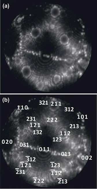
Figure 3. (a) Field ion microscope image of the apex of a sharply etched Tungsten tip (logarithmic scale). (b) Miller indices of the crystallographic surface planes at the apex.
Figure 3a shows a field ion microscope image of the apex of a Tungsten tip, recorded at a temperature of 30 K with a voltage of 7.4 kV applied to the tip. A long integration time of 5 min results in a high contrast image. The bright spots correspond to locations of high field intensity on the apex, i.e., to individual adatoms on the surface. Assuming that the flat image on the phosphor screen is formed by a projection of the surface from a point source at the center of the tip, a reconstruction of the curved apex surface is possible [Gault, 2012] and individual crystallographic planes at the apex can be assigned (see Miller indices in Fig. 3b).
Importantly for the use of these tip-shaped as electron emitters in ultrafast transmission electron microscopes, the FIM images allow for the determination of the local radius of curvature on the tips. This holds information about the most probable locations of electron emission. The radius of curvature can be estimated from the number of visible atomic steps between the adjacent plateaus of two crystallographic planes and the knowledge of the respective lattice constants. For example, in Fig. 3, local radii of curvature of 18.4 nm and of 9.6 nm are determined between planes (011) and (112) and between (222) and (211), respectively.
Conclusion
The field ion microscope presented here has enabled us to image the apex surface of sharply etched Tungsten nanotapers that are intended as emitters for time-resolved electron microscopy. The FIM yields images with atomic resolution, which allows reconstructing the 3D surface shape with its crystallographic planes. The knowledge of local radii of curvature on the apex will prove valuable information when evaluating new tips as well as novel sources of coherent electron beams regarding their suitability for ultrafast electron microscopy and diffraction.
References
- [1] J. Vogelsang, G. Hergert, D. Wang, P. Groß, and C. Lienau, Light: Sci. & Appl. 7, 55 (2018)
- [2] M. Gulde, S. Schweda, G. Storeck, M. Maiti, H. K. Yu, A. M. Wodtke, S. Schäfer, and C. Ropers, Science 345, 200 (2014)
- [3] B. Gault, M.P. Moody, J.M. Cairney, and S.P. Ringer, Atom Probe Microscopy, Springer (2012)
- [4] J.P. Ibe et al., J. Vac, Sci. Technol. A 8, 3570 (1990)
Contact
PD Dr. Petra Groß
Phone: +49 (441) 798 3490
E-mail: petra.gross@uni-oldenburg.de
Web:https://uol.de/uno
Prof. Dr. Christoph Lienau
Phone: +49 (441) 798 3485
E-mail: christoph.lienau@uni-oldenburg.de
Web:https://uol.de/uno
Prof. Dr. Sascha Schäfer
Phone: +49 (441) 798 3536
E-mail: sascha.schaefer@uni-oldenburg.de
Web:https://uol.de/und
Institute for Physics
Carl von Ossietzky University
26129 Oldenburg
Germany

