In selecting a scientific camera there are other parameters that should be assessed to ensure the camera can offer the best possible performance in the widest range of applications. These include:
- Sensor readout optimization options
- Cooling options
- Synchronization signals
- Computer interfacing options
To allow the camera to be optimized for the widest range of applications it is important to have options for the camera readout and these include;
- Sensor Preamp options
- Variable pixel speed options
- Variable vertical shift speed options
- Binning and sub image options
These options and the reason for their selection are explained in the following sections.
A CCD sensor can have a much larger dynamic range than can be faithfully reproduced with the current A/D converters and signal processing circuitry currently available in digital cameras. To access the range of signals from the smallest to the largest and to optimize the camera performance it is necessary to allow different pre-amplifier gains. Let's take the example of one sensor and it's various options to appreciate the issues and see how using different pre-amp gains allows us to make the best choices.
If we consider the DU920N-BV spectroscopy camera the sensor has a readout noise < 4e-.A single pixel has a full well capacity of 500Ke- and if we bin the sensor it has an effective full well capacity of 1,000Ke-. The single pixel dynamic range is 125,000 to 1 and the binned dynamic range is 250,000 to 1. A camera with a 16bit analog to digital converter (ADC) has only 65536 different levels so we are immediately stuck in a dilemma. The ADC cannot cover the full dynamic range of the CCD. If we set the gain of the pre amplifier of the camera to be 4e- then noise will be approximately 1 count but the ADC will saturate at ~262Ke-. If we set the gain of the pre amplifier of the camera to be ~16e- then ADC will then saturate at ~1,000Ke- but now the lowest level of signals will be lost within a single ADC count. The limited range of the ADC effectively creates a new noise source. The ADC produces discrete output levels and a range of analog inputs can produce the same output. If we consider the quantization noise that arises from the imperfect transformation of analog signals to digital signal sby the ADC the uncertainty of error produces an effective noise given by:
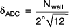
Where Nwell is the effective full well capacity of a pixel in electrons and n is the number of bits of the ADC. If we add this noise in quadrature with the noise floor of 4e- we can see this limits the dynamic range of the system.
You can immediately see unless the gain of the preamp is set sufficiently high the noise from the ADC significantly increases the overall system noise. To achieve the highest sensitivity or lowest noise it is important to have a preamplifier setting which allows the ADC noise to be negligible. This can be achieved by setting a gain where the read noise is much less than 1 count of the A/D (half in the case above). The next logical point to set the gain is to optimize the ADC to match the full well of a single pixel i.e. the highest count level equates to the full well depth.The third logical setting of the preamplifier gain is to match the highest ADC count to the full well depth of the readout register (typically 2 times the single pixel depth). This level allows the highest signal to noise ratio.
| Gain |
Saturation |
ADC Noise |
Total Noise |
Comments |
| 2e-/ADC |
~130,000 |
0.6 |
4.0 |
Highest sensitivity |
| 8e-/ADC |
~524,000 |
2.3 |
4.6 |
Best S/N ratio for single pixel |
| 16e-/ADC |
~1,000,000 |
4.4 |
5.9 |
Best S/N ratio for binned pixels |
The Horizontal Readout Rate defines the rate at which pixels are read from the shift register. The faster the Horizontal Readout Rate the higher the frame rate that can be achieved. The ability to change the pixel readout speed is important to achieve the maximum flexibility of camera operation. Slower readout typically allows lower read noise but at the expense of slower frame rates. Depending on the camera there may be several possible readout rates available.
The Vertical shift speed the time taken to shift the frame vertically by one row towards the shift register. The ability to vary the vertical shift speed is important for several reasons. It is possible using the different vertical speeds to better synchronise the frame rates to external events such as a confocal spinning disc. Faster vertical shift speeds also have benefits in lower clock induced charge especially for EMCCD's e.g.iXon3 EMCCD camera. A drawback with faster vertical shift speeds is that the charge transfer efficiency is reduced. This is particularly important for bright signals as a pixel with a large signal is likely to leave a significant charge behind which results in degraded spatial resolution. You may select a Vertical Shift Speed (the speed with which charge is moved down the CCD-chip prior to readout) from a drop-down list box on the CCD Setup Acquisition dialog Box. The speed is actually given as the time in microseconds taken to vertically shift one line, i.e. shorter times = higher speed. Slower vertical clocks ensure better change transfer efficiency but results in a slower maximum frame rate and possibly higher well depth. To improve the transfer efficiency the clocking voltage can be increased using the Vertical Clock Voltage Amplitude setting. However, the higher the voltage, the higher the clock-induced charge. The user must make a measured judgement as to which setting work best for their situation. At vertical clocks of 4µs or longer the "Normal" voltage setting should be suitable.
Increasing the frame rates can only be achieved by effectively reducing the total number of pixels to be read out. There are two principal ways of achieving higher frame rates, either by binning or by sub image or cropped mode readout. Binning is the process whereby charge from a group of pixels can be summed together. In addition to achieving faster frame rates this increases the signal to noise ratio but it also degrades the image resolution as the summed pixels act as one large super pixel. Adding pixels together before reading them out reduces the numbers of pixels. Sub image or cropped mode is the process whereby a portion of the active image is readout out or cropped and the surrounding extraneous image is discarded. The sub image region can be any smaller rectangular region of the sensor and the smaller the sub region the less pixels to be readout and consequently the faster the frame rates. It is possible to also combine the techniques of using a sub region and binning them to achieve even faster frame rates. Another way to achieve ultra fast frame rates is to use a special form of crop mode called Isolated crop mode to further speed up the frame rates in special circumstances. If only the bottom left corner of the sensor is illuminated the rest of the sensor can be ignored and as the sub image closest to the readout register is readout the camera does not need to discard the rest of the image prior to reading out the sub image again. This saves time and speeds the cropped mode up even faster.
Cooling the sensor reduces noise and this is very important for high sensitivity measurements. The camera performance improves with reducing temperature not just due to lower dark current but also due to reduced effects from blemishes. Cooling the sensor much lower than –100ºC is of limited benefit and below –120ºC many sensors no longer operate.Cooling can be achieved by either using proprietary thermoelectric coolers or Joule Thompson Coolers such as the Cyrotiger. Historically cooling of sensors has been accomplished with liquid nitrogen (LN2). The use of LN2 as a coolant is, at best, inconvenient. Maintenance, operating cost, availability at remote locations, and the hazardous nature of the material all combine to limit the practicality of a LN2-cooled device. The ability to operate the cooling at different temperatures is useful. At times when the highest sensitivity is required setting the temperature to the lowest possible is best. To operate the sensor for the best long term stability and lowest drift setting the temperature should be set at approximately three quarters of the lowest temperature possible. To operate the sensor at the most efficient power setting the sensor should be set to approximately half the minimum temperature.To cool the sensor it must be operated in a vacuum. To efficiently cool it, the sensor should be the coldest component in the camera, unfortunately that means if the sensor is not in a very good vacuum the sensor now becomes the surface of choice for condensates such as moisture and hydrocarbons. Condensates degrade the sensor and damage its performance particularly it's quantum efficiency. Andor has developed our proprietary UltraVac™ enclosure to ensure the highest vacuum possible and one that remains for a minimum of 5 years guaranteed.
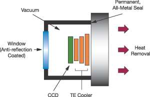
Our cameras are produced in our production facility in Belfast which boasts a Class 10,000 clean room, which is essential for building high quality, permanent vacuum systems - this means fewer than 10,000 particles of less than 0.5µm dimension per cubic meter. Andor’s innovative vacuum seal design means that only one window is required in front of the sensor enabling maximum photon throughput. This design is suited to high-end CCD cameras for operation in photon-starved conditions. An anti-reflection coating is also an option to further enhance performance and a MgF2 window is available for operation down to 120nm. We all know that it is more complicated than that. Pixel size needs to be taken into consideration, reduced dark current is the true goal and even that will differ for sensors and manufacturers, however it is worth looking at different cooling options so that we can best configure our system solution. In cooling the sensor it should be appreciated that the TE cooler removes heat form the sensor and now this heat energy must be removed from the camera to allow the camera to retain the sensor at the appropriate temperature. This can be achieved by either using air or water to remove the excess heat from the camera. Using air is a good and effective method of removing heat from your CCD.
Positive points of Air cooling:
- Convenient: not reliant on any extra power or equipment
- None of the problems or dangers associated with liquid nitrogen
- None of the problems concerning the use of cooling water below the ambient dew point
Negative points of Air Cooling:
- Detector design becomes large and bulky
- Power requirements will be greatly increased
- Vibrations from the fan could compromise measurements
Water is also a good and effective way to remove excess heat. The water acts as a medium to remove the heat from inside the camera head and the excess heat can then subsequently be transferred to air cooling. Water can come from any source of clean water such as the tap or from a water circulator.
Positive points of using a water circulator:
- This is a compact and effective cooling aid
- Once the water has been added to a circulator: no mains water supply is required making the unit very portable
- Condensation is not usually an issue
Negative points of using a water circulator:
- Addition of another piece of equipment to the system set-up
Water can also come from a water chiller. Water chillers can be used in a wider range of temperatures to achieve the best possible cooling performance. The chiller sets a reliable body temperature of the camera which reduces drift. An issue to be aware of however is that the temperature of the cooling water must not be below the dew point of the ambient atmosphere. For example, in a room at 25°C with 40% humidity the dew point is 8.5°C so cooling with 10°C water is fine. If you used water below 8.5°C then moisture will start to condense onto the electronics in the head and this can lead to serious damage.
It is often necessary to coordinate the reading of a camera with external hardware. Examples of external hardware are an Acoustic Optical switched laser source or be as simple as a mechanical shutter. Andor cameras have several mechanisms to allow this to happen. First the camera can be internally triggered i.e. the cameras acts as the master and sends out signals to allow other hardware be aware it is taking a scan. When running the camera sends a TTL pulse out on the ‘FIRE’ signal connector. The camera can be operated as a peripheral device and be externally triggered. In this case the camera waits for a TTL signal on the EXT TRIG connector before taking an exposure.
Cameras or for that matter PCs by themselves aren't especially useful. The value comes from being able to connect them and then using their respective properties to do so much more. Cameras can capture the images and the PC’s can convert these images into real information. We will review here the various interfaces that can be used to connect a camera to a PC.
PCI
USB
Firewire 1394
Internet
The original version of the Universal Serial Bus, known as USB 1.1, started appearing about in 2000. USB ports are now universal on new Windows and Macintosh computers. USB 1.1 moves data back and forth as fast as 12 megabits per second (Mbps). That's more than enough for many devices, but some - such as scanners, camcorders, external hard drives and external CD drives - benefit greatly from more speed. So an industry group called the USB Implementers Forum USB 2.0 as a second-generation standard. USB 2.0 is 40 times faster than its predecessor and is capable of moving data at a 480 Mbps.
The Firewire interface was developed by Apple Computers in the mid 1990’s and was adopted by an independent trade association called the 1394 Trade Association after the IEEE 1394 computer interface standard. The other major backer is Sony, using the i.Link name. Firewire can be operated as a synchronous device which allows high speed bandwidth for short periods of time. Recently introduced with 1394, data can now be transferred as fast as 800 Mbps, faster than USB 2.0. Apple and Sony put 1394 ports on all their computers; a few other manufacturers, notably Compaq, put 1394 on a few high-end models but the interface is not used as widely as USB 2.0.
The PCI (Peripheral Component Interconnect) bus was first introduced by Intel in 1991 to replace the ISA/EISA bus. The bus is not hot pluggable and involves opening the computer to obtain access to the slots. It was later taken over by the PCI Special Interest Group (PCI-SIG) who revised the protocol in 1993. The bus offers a total available bandwidth of 1Gigabit/s but this is shared between slots which mean that high demand devices can quickly saturate the bandwidth. In 1997 this problem was partially alleviated by implementation of a separate AGP slot (Accelerated Graphics Port) with dedicated bandwidth. Other steps were also taken at the chip level along with integrated components, which helped to extend PCI's viability. However, with the advent of SATA, RAID, Gigabyte Ethernet and other high-demand devices, a new architecture is required. The PCI bus is expected to be phased out in 2006 to make way for the PCI express bus.
PCI Express is a scalable I/O (Input/Output) serial bus technology set to replace parallel PCI bus which came standard on motherboards manufactured from the early 90's. In the latter part of 2005, PCI Express slots began appearing alongside standard slots, starting a gradual transition. PCI Express has several advantages, not only to the user but to manufacturers. It can be implemented as a unifying I/O structure for desktops, mobiles, servers and workstations, and it's cheaper than PCI or AGP to implement at the board level. This keeps costs low for the consumer. It is also designed to be compatible with existing Operating Systems and PCI device drivers.PCI Express is a point-to-point connection, meaning it does not share bandwidth but communicates directly with devices via a switch that directs data flow. It also allows for hot swapping or hot plugging and consumes less power than PCI.The initial rollout of PCI-Express provides three consumer flavors: x1, x2, and x16. The number represents the number of lanes: x1 has 1 lane; x2 has 2 lanes, and so on. Each lane is bi-directional and consists of 4 pins. Lanes have a delivery transfer rate of 2 Gbs in each direction for a total of 500 GBs per lane.
| PCIe |
Lanes |
Pins |
Speed |
Purpose |
| x1 |
1 |
4 |
4 Gbs |
Device |
| x2 |
2 |
8 |
8 Gbs |
Device |
| x16 |
16 |
64 |
64 Gbs |
Graphics Card |
The 16-lane (x16) slot replaces the AGP for PCIe graphics cards, while the x1 and x2 slots will be used for devices. As graphic demands increase, x32 and x64 slots will be realized, and future versions of PCIe are expected to drastically increase lane data rates.
PCI Express is not to be confused with PCI-X, used in the server market. PCI-X improves on standard PCI bus to deliver a maximum bandwidth of 1GBs. PCIe has been developed for the server market as well, initially with the x4, x8 and x12 formats reserved. This far exceeds PCI-X capability.
Ethernet was originally developed by Xerox Corporation to connect computers to printers. Ethernet uses a bus or star topology to connect computers and peripherals and supports data transfer rates of 10 Mbps. The Ethernet specification served as the basis for the IEEE 802.3 standard, which specifies the physical and lower software layers. It is one of the most widely implemented LAN standards. A newer version of Ethernet, called 100Base-T, supports data transfer rates of 100 Mbps and the latest version, Gigabit Ethernet supports data rates of 1 gigabit (1,000 megabits) per second.

