
Resources
 Part of the Oxford Instruments Group
Expand
Collapse
Part of the Oxford Instruments Group

Application Notes
Published: 20 Sep 2023 · Last updated: 20 Sep 2023
Electronic components are at the heart of many modern-day devices and are relied upon to perform consistently to stringent specifications. Many of the structures within printed circuit boards (PCBs) are present on a µm to nm scale. Ensuring that these often complex components have been built to design both in terms of structure and composition is key, as is the investigation and diagnosis of failures or contamination. As devices become ever more complex, with smaller scale structures, scanning electron microscopy (SEM) plays an increasingly important role in component quality control.
There are many ways that SEM-based analysis may be used to investigate electronic components. Examples include:
As alluded to above, structure exists at many scales in electronic devices. This means that spatially distributed information is essential for solving problems. Given the multiple different materials that are typically used in a PCB, a combination of backscattered electron (BSE) and compositional X-ray imaging provides the most useful, intuitive and time-efficient way of understanding a sample.
This information has historically been acquired in a sequential way, with electron images acquired first – giving a good understanding of the layout of a sample – followed by compositional X-ray data. In this approach, the operator's understanding of the electron image guides the decision as to where and when to collect compositional data. Consequently, when a feature of particular interest is not immediately visible in the electron image, it may easily be missed, resulting in compositional data not being acquired. Furthermore, if multiple sources of contamination are present within a sample, they may be mistaken as being from the same source, if electron imaging only is used.
The solution to this is to acquire both electron and compositional images simultaneously with Unity in the first step of the analysis workflow, using a new technique called BEX imaging. Using BEX, the Backscattered Electron and compositional X-ray (BEX) data are acquired together, thus removing many of the decisions on what to analyse compositionally and where. Live maps are shown as the operator moves across the sample, giving an instant understanding of exactly what is present. A screenshot of this process is shown in Figure 1.
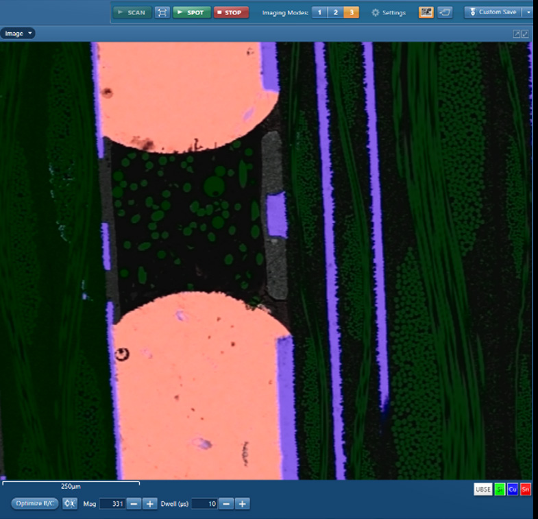
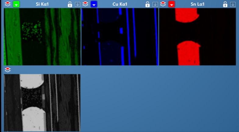
Figure 1. Single Field BEX view of PCB Cross Section - Layered Image (top) and individual element maps (bottom).
Once a site of particular interest has been identified – potentially showing a key feature in the sample – e.g. the site of a failure, the next step is often to output that data so that it can be easily reported on. When using Unity, one can take a high-quality image using a single click from any location of interest. This image may be sufficient to report on the sample, and collecting it could be the end of the job. An example of a 4K image captured with this method is shown in Figure 2.
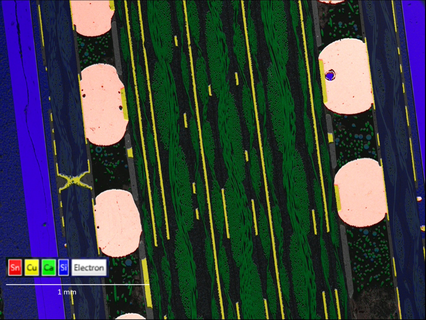
Figure 2. 4k resolution custom cartography capture of a single, low-mag field of view acquired with simultaneous BSE and X-ray (BEX) imaging
The approach can be extended from a single field of view to a much wider area across the sample by making use of cartography mode – a method where the BEX approach combined with Unity's very high data acquisition rates are used to particularly advantage to acquire very detailed, combined electron image and compositional X-ray maps more quickly than has previously been possible. The setup of these large area runs is very rapid and is performed by simply dragging over the area of interest on the screen. A run is then started with a single click. In this case, an area of 44 fields was defined to study a large proportion of the cross-sectioned PCB sample including multiple solder bumps – Figure 3. The resulting map is shown in Figure 4.
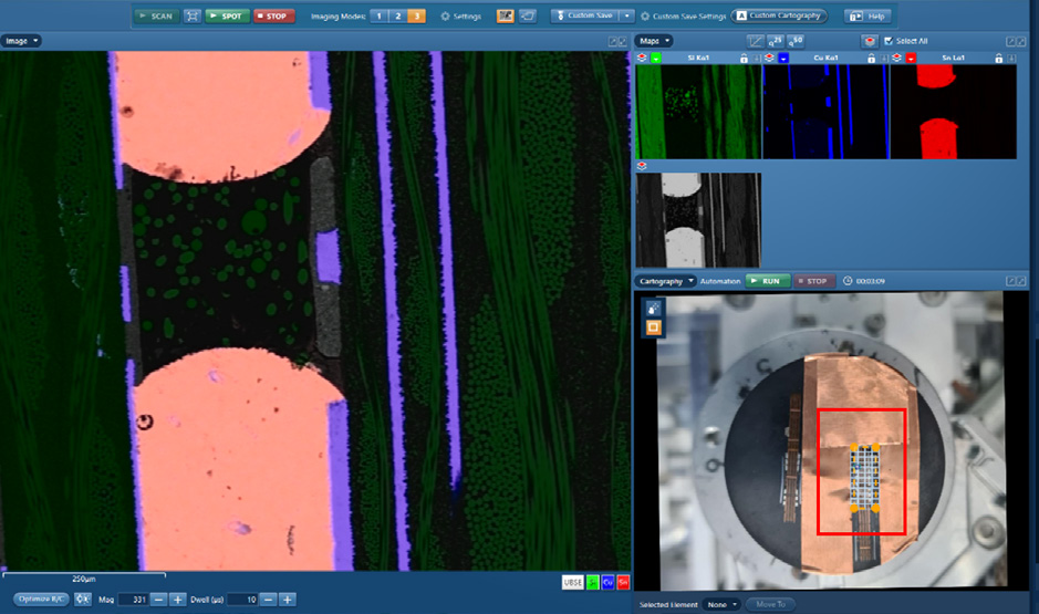
Figure 3. Setup of a BEX Map with Cartography Mode. A rectangle (within the red box highlight) is drawn over the area of interest in the sample. The mapping then begins as soon as the run button is pressed.
The map is taken over a large area of 4.2 x 8.2 mm and shows various different PCB layers and solders, and was mapped in just over 2 minutes. The map confirms that the PCB board meets specification in terms of the number of Cu layers and no cracking or voids were found in the solder bumps. In one case, a large piece of Si was found in a solder bump (seen at the top left of the image) and this was reported back to the owner of the sample for interpretation. No signs of current or voltage stress were found.
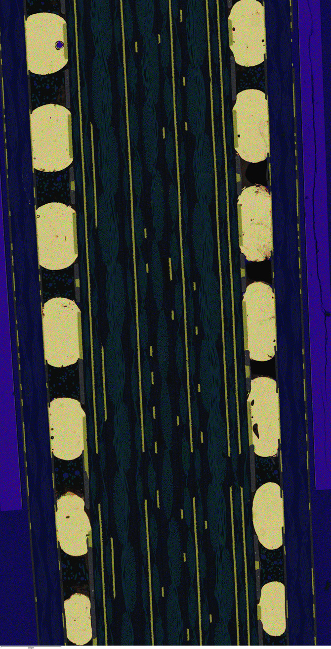
Figure 4. Large Area BEX Map of the cross-section of the PCB. The map consists of 44 fields and was collected in 2 minutes 7 seconds.
Unity imaging provides both imaging and compositional information that are important for electronics devices characterisation. Quick and reliable analysis of the different device failures and inspection of various electronic components, to check if they meet product specification, is an easy task now using high-throughput cartography imaging with Unity. These findings can help eliminate failure in the devices, weak points or production-related deficiencies.

© Oxford Instruments 2026