Application Notes
AZtecCrystal MapSweeper e-book
Published: 11 Aug 2023 · Last updated: 11 Aug 2023
Tags: EBSD
MapSweeper Explained
Conventional electron backscatter diffraction (EBSD) and transmission Kikuchi diffraction (TKD) utilise the Hough Transform to detect Kikuchi bands in each diffraction pattern, from which the best matching phase and crystallographic orientation are calculated. However, although fast and highly optimised, Hough-based indexing has limitations in terms of precision, pattern deconvolution (such as at grain boundaries) and effectiveness for indexing poor quality patterns, as is typical from highly-deformed materials.
AZtecCrystal MapSweeper is an offline reanalysis tool that uses advanced pattern matching techniques to improve the quality of EBSD / TKD datasets. Pattern matching methods are far superior to Hough-based indexing for the analysis of deformed or nanocrystalline materials, but the pattern matching tools in MapSweeper also have many other benefits, including improved angular precision, better phase discrimination and the measurement of new information, such as crystal polarity.
Diffraction Pattern Simulation
A master simulation pattern needs to be created for each phase prior to the pattern matching reanalysis: from each master pattern, simulated EBSD / TKD patterns (or "templates") are created as and when needed. MapSweeper includes a fully flexible master simulation creation tool:
- Choose between kinematic, 2-beam or many-beam dynamical electron diffraction models
- Create master simulations in just minutes
- Re-use master simulations for all subsequent analyses with the same phase and beam energy
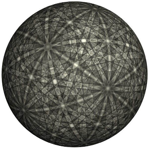
Pattern Matching
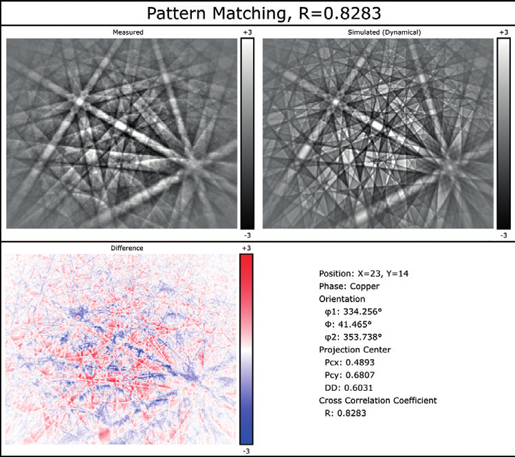
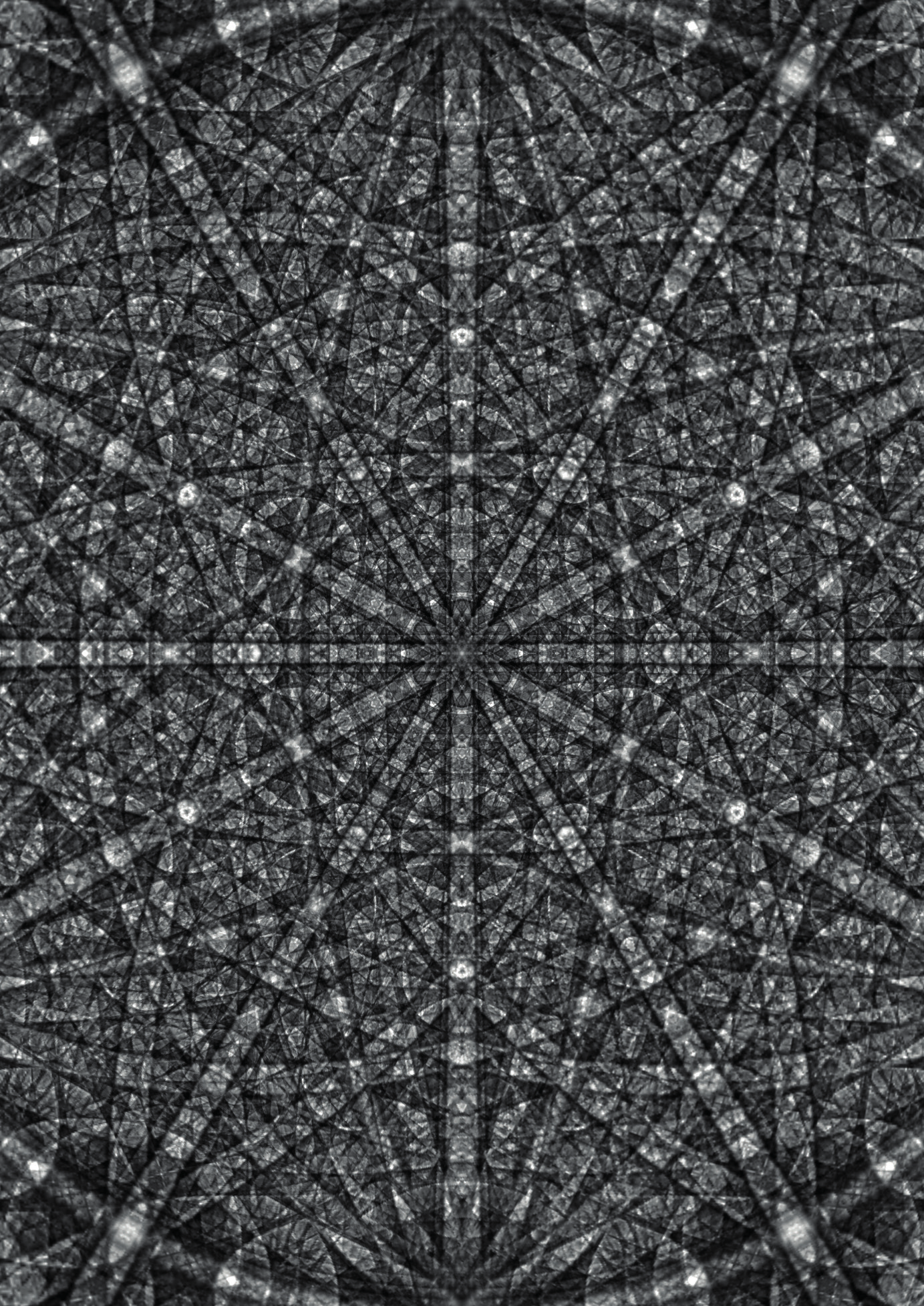
Each experimental EBSD / TKD pattern is matched against multiple simulated templates, each derived from the relevant master pattern using refined pattern projection parameters. The images are correlated using the normalised cross correlation coefficient (R), a robust metric for measuring image similarities. The phase and orientation of the simulated template that results in the highest R value is accepted as the optimum solution.
Dataset Reanalysis
MapSweeper has multiple "sweep" modes that apply pattern matching techniques to each EBSD / TKD dataset. These can be combined with each other to deliver optimum quality data from any material, whatever the application.
- Indexing – a "brute force" approach ignoring any previous phase and orientation data, using a new approach called Dynamic Template Matching (patent pending)
- Refinement – a fast, hybrid method, building on prior phase and orientation data, that enhances data quality (e.g. precision or phase discrimination) or provides new information (e.g. polarity)
- Repair – a hybrid method to remove isolated errors and increase indexing hit rates without requiring a full indexing approach (patent pending)
- Indexing – a “brute force” approach ignoring any previous phase and orientation data, using a new approach called Dynamic Template Matching (patent pending)
- Refinement – a fast, hybrid method, building on prior phase and orientation data, that enhances data quality (e.g. precision or phase discrimination) or provides new information (e.g. polarity)
- Repair – a hybrid method to remove isolated errors and increase indexing hit rates without requiring a full indexing approach (patent pending)
MapSweeper Explained: Indexing
For an electron backscatter diffraction (EBSD) or transmission Kikuchi diffraction (TKD) dataset, if the initial indexing (e.g. using the Hough-transform indexing approach) is poor, it is possible to re-index each diffraction pattern using novel pattern matching techniques. This usually involves comparing each experimental EBSD pattern with multiple simulated patterns that correspond to every possible crystallographic orientation and every candidate phase. The simulated pattern that matches best with the experimental pattern is then selected as the correct solution and the corresponding phase and orientation are stored.
Sometimes referred to as "brute force indexing", this approach was first proposed in 2015, as the dictionary indexing (DI) method [1]. However, the DI approach is laborious, requiring the creation of a library of potentially millions of simulated patterns (or "templates") for each phase, depending on the desired angular precision and the crystal symmetry of each phase. This library would need to be created for each experiment, a process usually taking many hours, and the subsequent retrieval of each template and correlation against the experimental patterns would also typically be slow, limited to just a few analysis points per second.
AZtecCrystal MapSweeper utilises a new approach to brute force indexing, a technique called "Dynamic Template Matching" (patent pending), which may be considered similar to the DI method but without the need for a template library. In this technical note, the fundamentals and benefits of the DTM method are explained.
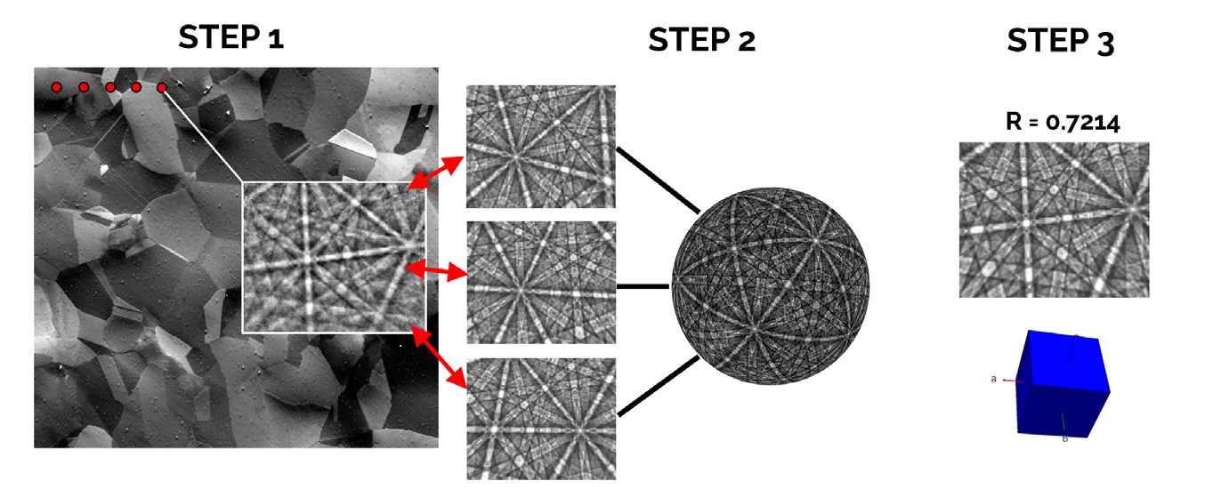
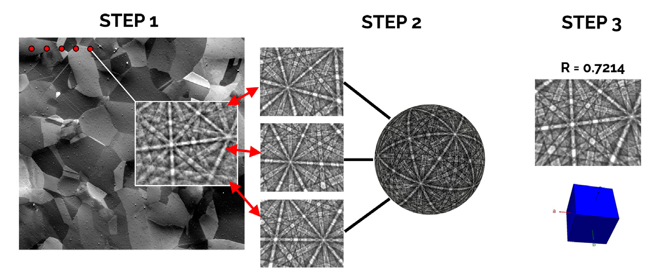
The process of Dynamic Template Matching. 1 – collect and store experimental diffraction patterns. 2 – generate templates for all orientations / phases and match against each experimental pattern. 3 – select the solution with the highest normalised cross correlation coefficient, refine the orientation and save the result.
Dynamic Template Matching
Dynamic Template Matching (DTM) is, as the name implies, a dynamic approach to brute force indexing using pattern matching. Unlike dictionary indexing, DTM does not require the generation of a large library of simulated pattern templates, but instead creates (and discards) templates as they are required. There are multiple benefits to this more dynamic approach:
- No requirement to pre-calculate a large library of templates for each experiment
- The geometry calibration parameters can be adjusted for each position in the mapped area
- The resolution and orientation spacing of each template can be varied
- Each solution can be quickly refined to a desired level of precision
- Faster speeds than DI – typically 10s – 100s patterns per second (depending on computing power and crystal symmetry)
The step-by-step process of DTM is quite simple:
Step 1: Analyse the sample using EBSD or TKD, and store the diffraction patterns at each point.
Step 2: From a pre-calculated master simulation pattern for each candidate phase, individual templates are created for all possible crystal orientations, and these are matched against the experimental diffraction pattern at every point in the dataset. For speed, this is usually performed at a low resolution (e.g. 40 x 30 pixels). The templates are generated using the projection geometry calibration at each point and are discarded immediately after use.
Step 3: The orientation and phase corresponding to the template that has matched best to the experimental pattern (i.e. with the highest normalised cross correlation coefficient, R) is accepted as the correct solution (assuming R exceeds a user-defined minimum threshold). This orientation is then refined using a higher pattern resolution and the end result is saved.
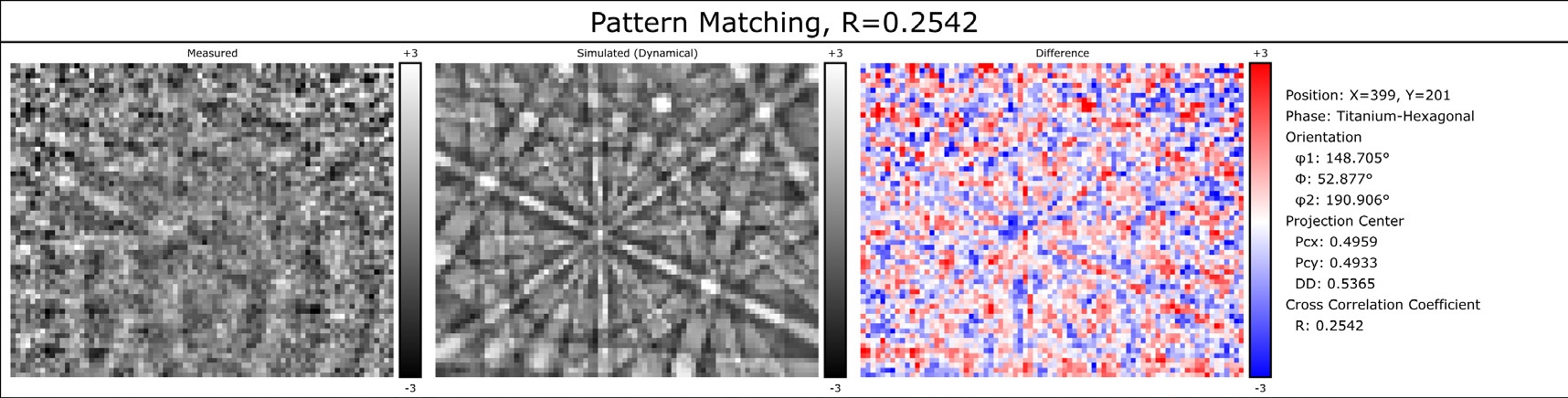
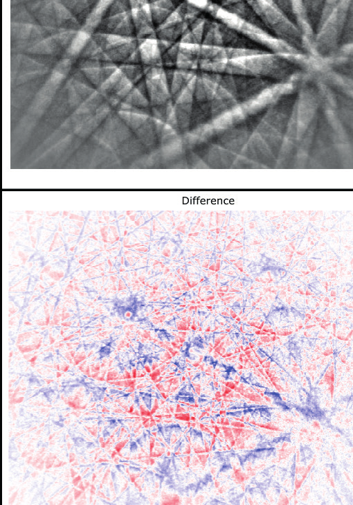
Results of DTM indexing of a poor quality EBSD pattern from a highly deformed Ti grain. Left – experimental pattern; centre – best matching simulated template; right – difference between the 2 patterns.
The DTM approach will always find a solution. This means that even for very poor-quality patterns that could not be indexed using the Hough-transform approach, DTM will provide phase and orientation data. An example is a diffraction pattern collected from a cold-deformed Ti alloy. The lattice distortion has blurred out the Kikuchi bands, making indexing using conventional band detection techniques impossible. However, indexing using the DTM approach is robust, with an R value significantly exceeding the standard default threshold of 0.15.
The fact that DTM indexing will always find a best matching solution is also a weakness; any image, whether it is a noisy diffraction pattern or a random photograph, will have a best solution. Therefore it is important that a robust image similarity metric such as the normalised cross correlation coefficient is used, and that a suitable minimum threshold value is applied in order to filter out unreliable solutions.
The benefits of the improved indexing capability of DTM are demonstrated in the following example, taken from an impact-deformed diamond sample measured using TKD. The initial indexing rate was only 51% but after reprocessing using DTM in MapSweeper, the final indexing rate was 98%. This then enables a rigorous characterisation of the grain structures, boundary types and dislocation content.
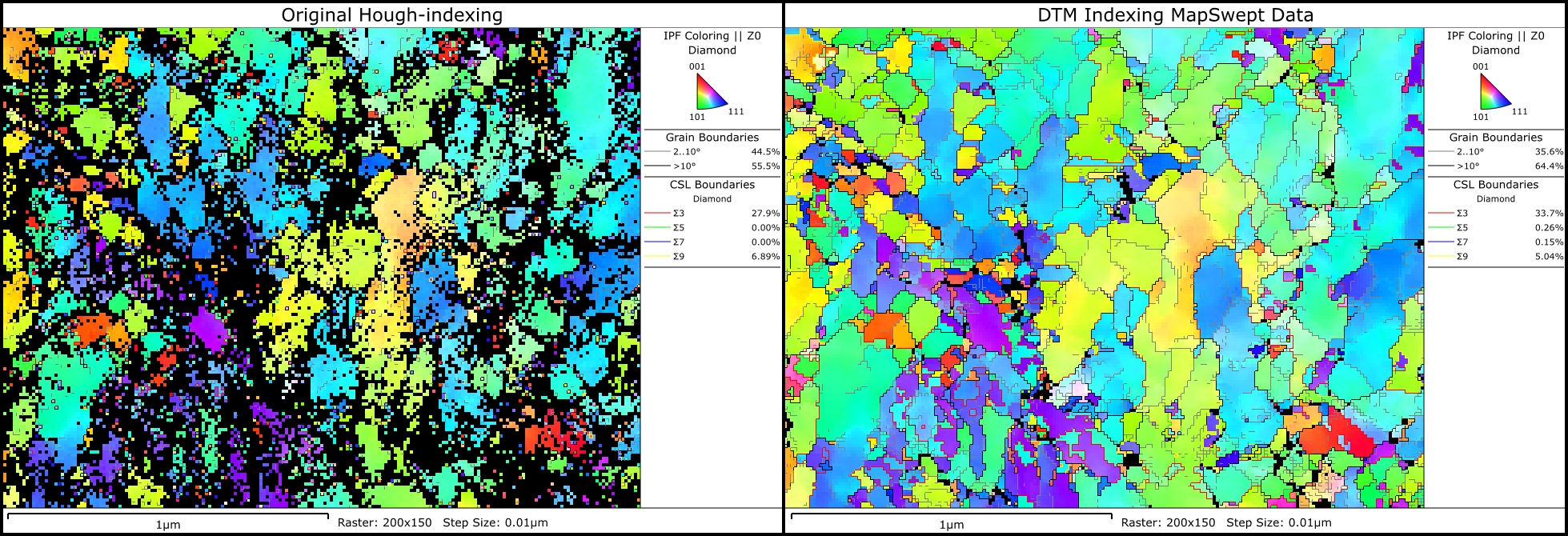
TKD orientation maps from an impact diamond sample. Left – initial results using Hough-based indexing, with 51% indexing rate. Right – results after reprocessing using DTM in MapSweeper, with 98% indexing rate. Scale bars mark 1 µm.
Summary
One of the most powerful advantages of pattern matching is its ability to index low quality diffraction patterns. Previous methods, such as DI, highlighted this potential but were time consuming and cumbersome to use. In AZtecCrystal MapSweeper, a new approach to indexing, Dynamic Template Matching, is utilised, and this enables effective re-indexing of challenging datasets with minimal set-up time and with exceptional results.
References
- Y. H. Chen, S. U. Park, D. Wei, G. Newstadt, M. A. Jackson, J. P. Simmons, M. De Graef & A. O. Hero, (2015). "A dictionary approach to electron backscatter diffraction indexing". Microscopy and Microanalysis, 21(3), 739–752.
Technical Note: MapSweeper Explained — Refinement
The use of pattern matching techniques to improve electron backscatter diffraction (EBSD) datasets involves much more than just "brute force" indexing. Most EBSD (or transmission Kikuchi diffraction – TKD) datasets that have been indexed using conventional Hough-transform band detection methods have a high indexing rate and contain sufficient information to provide most of the relevant microstructural parameters, such as grain size, texture and boundary population statistics. It makes little sense to discard these data and to reprocess each EBSD pattern using potentially time-consuming pattern matching methods.
In such cases, a hybrid method of pattern matching is a more intelligent approach. Here, the original phase and orientation data are used to inform the pattern matching process, so it is only necessary to create simulated pattern templates for a very restricted set of phases and orientations for each measurement point. This refinement approach is therefore much quicker than a brute force method, such as dictionary indexing or Dynamic Template Matching, and results in significantly improved data quality. In AZtecCrystal MapSweeper, the Refinement sweep uses hybrid pattern matching methods to enhance each dataset in multiple ways, as described in the following sections.
Improved Angular Precision
The angular precision or resolution of conventional EBSD / TKD indexing is typically in the range of 0.2 – 1°, although real-time solution refinement methods, such as AZtec's patented Refined Accuracy, can improve this precision down below 0.05°. Improved angular precision has significant benefits, especially for the characterisation of dislocations and low angle boundaries.
In AZtecCrystal MapSweeper, the Refinement sweep uses pattern matching methods to improve the angular resolution of EBSD and TKD datasets as follows:
- Hybrid pattern matching based on original phase and orientation data
- Rapid refinement of orientation using a Nelder-Mead optimisation approach
- Improved cross correlation coefficient (R) values
- Orientation precision down to <0.01° (depending on EBSD pattern quality)
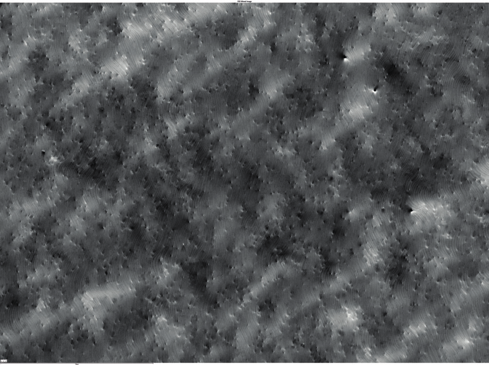
The example shows how MapSweeper Refinement can be used to resolve individual threading dislocations in a GaN thin film, with improved classification of dislocation type.
 Improved Phase Discrimination
In some materials, there exist phases that share a similar crystallographic structure, producing EBSD patterns that may be challenging to index correctly. X-ray compositional data or the relative widths of Kikuchi bands in the EBSD patterns can be used to improve phase separation, but only in certain cases.
The Refinement sweep in MapSweeper enables the use of hybrid pattern matching for a more robust discrimination between phases:
- Similar phases are grouped by the user to trigger further examination
- Patterns initially indexed as a grouped phase will be matched against simulated templates for all phases in the group
- The solution with the highest R value is used to determine the correct phase
- Rapid process that can separate phases with <1% unit cell variation (depending on pattern quality)
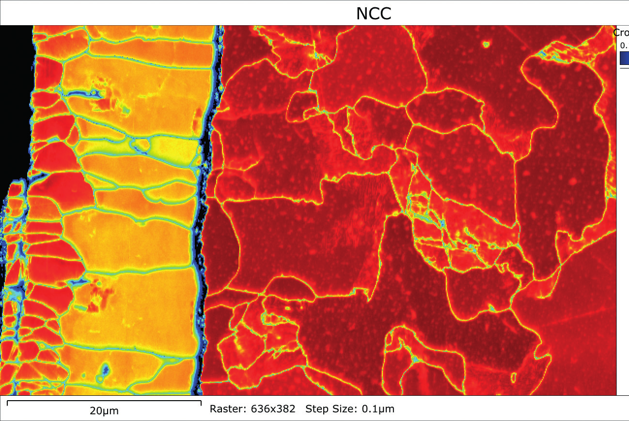
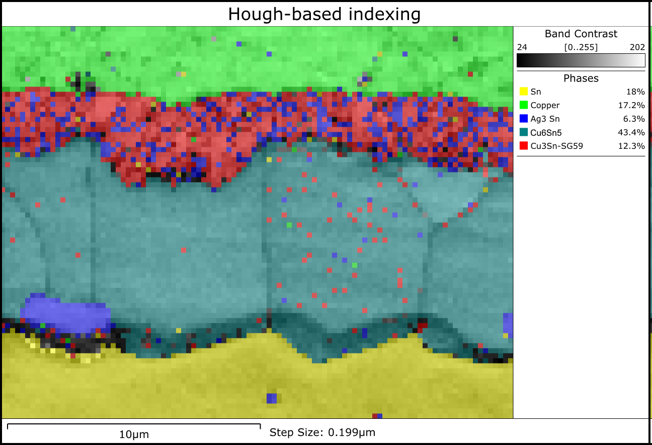
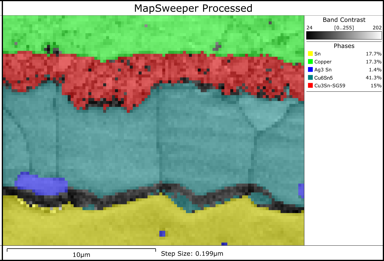
The Refinement sweep can be used to separate phases in many complex materials, including in steel oxide scales (e.g. cubic ferrite (Fe), wüstite (FeO) and magnetite (Fe3O4)) or, in the case shown, in micro-solder bumps in electronics components (e.g. orthorhombic Ag3Sn and Cu3Sn).
 Resolving Pseudosymmetry
Pseudosymmetry is the name given to a crystal structure that almost has a higher symmetry than its recognised space group. This results in 2 or more crystallographic orientations producing diffraction patterns that are very similar and may be difficult or impossible to separate using conventional EBSD indexing methods. Resulting datasets will include many mis-indexed points, and this will impact boundary, grain size and texture measurements.
The Refinement sweep in MapSweeper can correct for misindexing caused by pseudosymmetry, in the same way as for phase discrimination:
- The user defines the pseudosymmetry relations for the phase in question
- MapSweeper will match against all pseudosymmetry-related orientations
- The solution with the highest R value will be selected
- Rapid process that can resolve <1% lattice changes
The example shows a CuInSe2 solar cell sample that has a strong pseudosymmetry, as the tetragonal structure is only 0.5% away from having cubic symmetry.
 Measuring Polarity / Inversion Domains
In certain non-centrosymmetric materials, such as GaN, GaP and ZnO, a change in crystal polarity (or inversion) can result in very small changes in the diffraction pattern. These changes cannot be resolved using conventional indexing methods but, if the EBSD pattern quality is high enough, they can be measured using pattern matching approaches. Since the polarity of many materials, especially the wurtzite semiconductors, has a significant impact on the electronic and optical properties, being able to measure the polarity and to map individual polarity or inversion domains is a powerful new application of EBSD.
For relevant phases, the Refinement sweep in MapSweeper enables the polarity or inversion of each EBSD pattern to be tested using the rapid hybrid pattern matching approach.
 Summary
The hybrid pattern matching tools that make up AZtecCrystal MapSweeper's Refinement sweep enable significant enhancement of EBSD and TKD datasets. The benefits include improved angular precision, better phase discrimination, the removal of pseudosymmetry-related indexing errors and the measurement of crystal polarity or inversion.
Technical Note: MapSweeper Explained — Repair
No electron backscatter diffraction (EBSD) or transmission Kikuchi diffraction (TKD) dataset is perfect. Invariably there will be patterns that could not be indexed (such as at grain boundaries or voids), and there may also be others that are incorrectly indexed resulting in the wrong phase or orientation. It is convention to filter out these errors and to remove non-indexed points from a dataset using well-established clean-up routines, but this duplicates data and may result in the removal of valid measurements.
Pattern matching (PM) techniques are able to index successfully poor-quality EBSD / TKD patterns and to improve phase and orientation measurement reliability, but "brute force" PM indexing methods are relatively slow. A smarter approach is to use hybrid PM, where the initial orientation and phase data are used to inform the PM process.
The Repair sweep in AZtecCrystal MapSweeper is a hybrid PM method for improving EBSD and TKD datasets without requiring a full re-indexing approach. In this technical note, the benefits of the Repair sweep compared to existing data cleaning methods are explained.
Improving the Indexing Rate
Most non-indexed measurements occur at grain boundaries, where different diffraction patterns are superimposed, or in locations that give no diffraction pattern at all (such as in voids or off the edge of the sample). The Repair sweep in MapSweeper attempts to index patterns that were not initially indexed, using information from surrounding pixels; this approach does not duplicate data or generate results where there should not be any:
- The EBSD / TKD patterns at non-indexed points (above a defined pattern quality) are matched against simulated templates using the phase and orientations of every indexed neighbour point
- The best matching solution (with the highest normalised cross correlation coefficient, R) is then further refined using a Nelder-Mead optimisation approach
- The new, refined solution is accepted if the R value exceeds a threshold limit
- Subsequent passes can iteratively index remaining non-indexed points
The Repair sweep significantly improves the indexing hit rate in datasets whilst retaining data fidelity and quality. In many cases, the Repair sweep will be used in tandem with a Refinement sweep, ensuring high quality data across all measurement points. An example of how a repair sweep can enhance the indexing rate in a TKD dataset collected from a nanocrystalline Al sample is shown below.
Correcting Indexing Errors
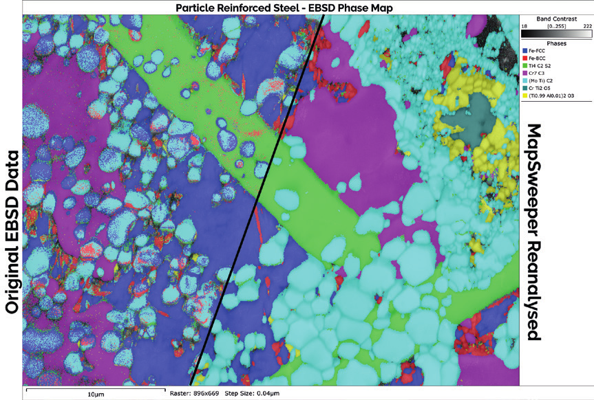
Isolated indexing errors can be common in EBSD and TKD datasets, producing single pixels or small clusters of pixels with different phase or orientation values compared to their neighbours. Conventional data cleaning methods will often be used to replace such measurements with a duplicate, representative neighbour value, but there are cases where the "errors" are in fact valid measurements (such as precipitates or single, small grains).
The Repair sweep in MapSweeper can test each small cluster and either verify (and improve) the original result, correct it to a result similar to a neighbouring point or, if there are no sufficiently close matching templates, remove the result altogether:
- Small pixel clusters are tested against simulated templates derived from the original and neighbouring measurements
- The best matching result (highest R value) is subsequently refined using a Nelder-Mead optimisation approach
- The result is only accepted if R exceeds a predefined threshold level
- Ensures consistently correct measurements with no data duplication
The example below shows a high-C steel that has been mapped, with numerous isolated errors in phase assignment (as well as orientation, not shown here). Following the Repair sweep, these errors have either been corrected or have been validated as very small 2nd phase grains (Fe carbides or retained austenite). In addition, the overall indexing rate has been significantly improved.
 Summary
The Repair sweep in AZtecCrystal MapSweeper is a smart, hybrid pattern matching tool that can rapidly enhance EBSD and TKD datasets. The method increases the indexing rate without data duplication, and removes isolated indexing errors, by use of neighbouring pixel data. The outcome is a significant improvement in EBSD and TKD data quality without requiring more time-consuming brute force indexing methods.
Application Note: Characterising Extreme Deformation in a Failed Al Alloy
Introduction
Unexpected metallurgical failure is extremely costly, either due to the additional costs of replacement parts and increased downtime, or due to more catastrophic consequences. Understanding the causes of failure is therefore a critical process; this will often involve microstructural characterisation in order to reveal the processes that lead to the part failure or to understand the mechanisms of the failure itself.
Although electron backscatter diffraction (EBSD) has been used as a key failure analysis tool for many years, the successful measurement of highly deformed materials is challenging, especially for conventional indexing using the Hough transform approach. In addition, the presence of brittle intermetallic phases is often a cause of failure, so it is critical that these phases are reliably measured during EBSD characterisation.
In this regard, EBSD pattern matching methods can be transformative; not only are they much better at successfully indexing diffraction patterns from highly deformed structures, but they can result in improved angular precision as well as more robust separation of phases, especially those that share similar crystal structures. In this application, the benefits of AZtecCrystal MapSweeper for the successful analysis of a failed Al alloy are demonstrated.
Sample and Experimental Details
A failed pole section made from a 7xxx series Al alloy was sectioned and mounted for analysis in the scanning electron microscope (SEM). The surface was prepared for EBSD using a vibratory polisher and then characterised using a field emission gun SEM, equipped with a Symmetry S3 EBSD detector and operating with a beam current of 24 nA and a 20 kV accelerating voltage. EBSD patterns were collected in Symmetry's "Speed 2" mode (156 x 128 pixel resolution) at rates between 180 and 470 patterns per second, were indexed using conventional Hough-based indexing in the AZtec software and then were stored for subsequent reanalysis. Two areas were analysed: a larger region (~300 x 250 µm) adjacent to the fracture surface at a measurement step size of 200 nm, and a smaller area (~50 x 50 µm) in a highly-deformed zone, with a 100 nm step size.
The data were reprocessed using AZtecCrystal MapSweeper, using dynamical simulations with Gaussian weighting of each pattern (to assign greater importance to the centre of each pattern, where the signal to noise ratio is higher). For the smaller, higher resolution dataset, the initially non-indexed points were indexed using Dynamic Template Matching (DTM) – as can be seen from the example, even very poor EBSD patterns can be effectively indexed using DTM, enabling high quality data from the most deformed regions of the sample.
Following DTM indexing, all points were analysed using MapSweeper's Refinement Sweep (to improve the angular precision of each measurement) and Repair Sweep (to correct isolated indexing errors and to improve the overall indexing rate). For the larger dataset, only the faster Refinement and Repair sweeps were carried out, enabling full enhancement of the ~1.8 M point dataset in approximately 90 minutes. In all cases, patterns were matched against simulated templates for 3 separate phases: Al, MgZn2 and Al7Cu2Fe.
Results
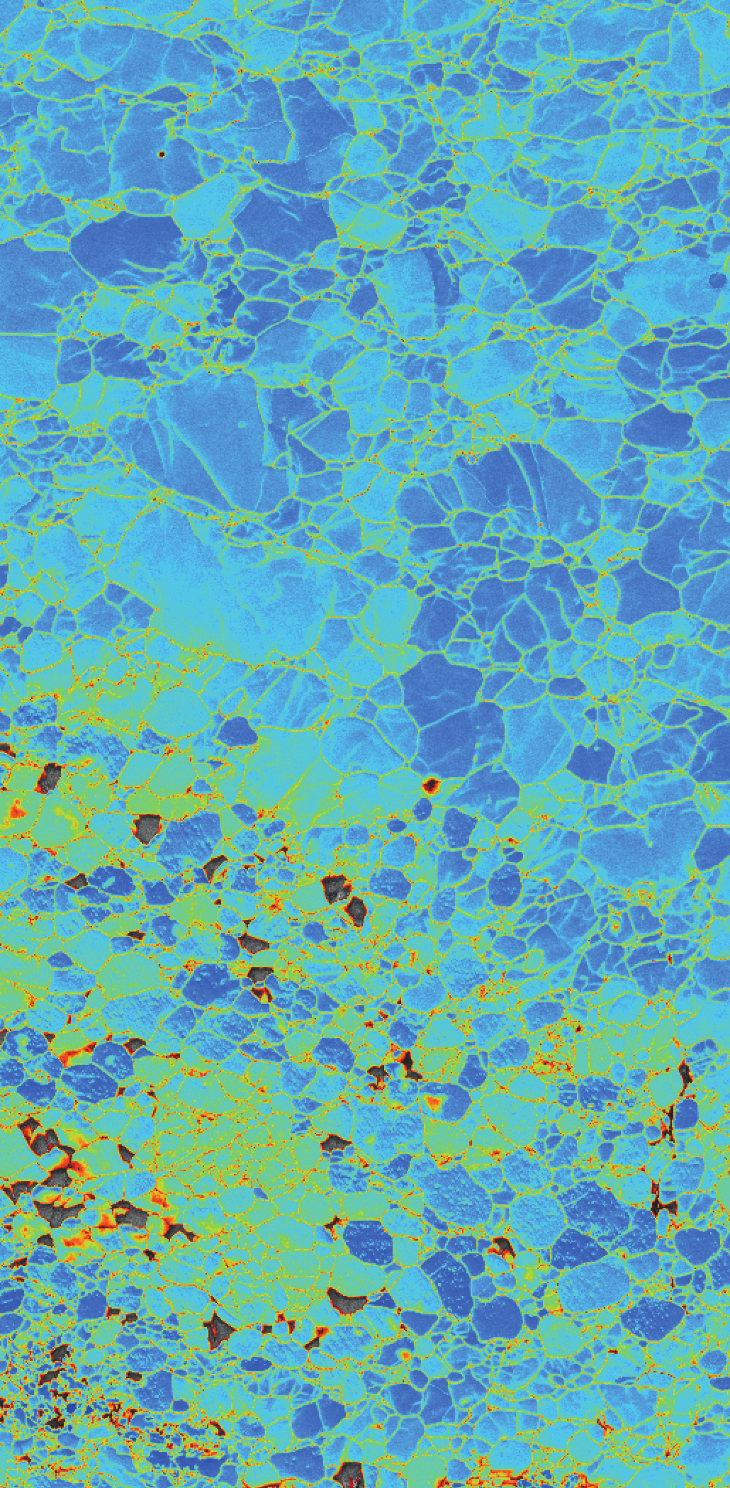
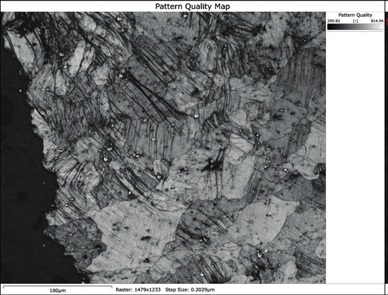
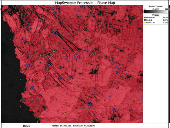
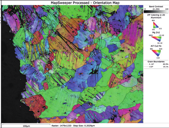
In the highly-deformed, smaller area, the initial indexing rate using the Hough-transform approach was only 70.5%. Following reprocessing using MapSweeper, the indexing rate increased to 96.9% (note that points with a normalised cross correlation coefficient below 0.15 were assigned as non-indexed). This enabled a more rigorous examination of the highly deformed areas, characterised by significant grain size refinement as well as increased defect densities, as shown by the Kernel Average Misorientation (KAM) maps. The improved data quality also highlights the brittle nature of the intermetallic phases and localised strain in the surrounding Al matrix.
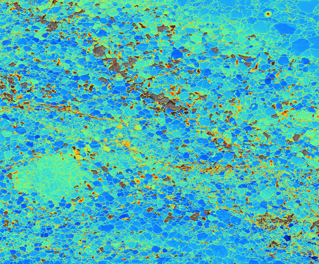
 In the larger analysis area, the indexing rate increased from 77% to >93% following the MapSweeper reprocessing (excluding the sample mount). This additional information, right up to the fracture surface itself, highlights once again the benefits of MapSweeper for characterising highly deformed regions. In this area, the prevalence of numerous slip bands in the Al matrix, as well as increased dislocation densities surrounding the intermetallic phases, help with the interpretation of possible failure mechanisms in this sample.
 Summary
The pattern matching methods implemented in AZtecCrystal MapSweeper are ideal for the effective characterisation of highly deformed materials. In this failed Al alloy sample, MapSweeper has enabled a rigorous examination of the most deformed regions close to the fracture surface itself. Not only does DTM indexing deliver high quality information from areas that have undergone significant grain size reduction, but MapSweeper's Refinement and Repair sweeps enhance both the angular precision and the phase discrimination within these datasets. The results indicate the importance of brittle intermetallic phases, concentrating strain in the surrounding Al matrix and potentially resulting in crack initiation, prior to failure.
Application Note: Unlocking the Secrets of Nanoscale Structures in Fault Rocks
Introduction
The microstructures that are formed during in geological fault zones during earthquakes are very challenging to characterise effectively. Depending on the pressure, temperature and strain rate, the resulting microstructures can be typified by very fine grained, dynamically recrystallised regions ("mylonites") or by brecciated material, potentially with veins of quenched melt rock caused by frictional heating ("pseudotachylites"). There have been numerous studies using electron backscatter diffraction (EBSD) to characterise mylonite microstructures, but pseudotachylites are significantly more challenging – mineral fragments are often highly deformed, extremely fine grained (e.g. <5 µm grain diameter) and surrounded by an amorphous, glassy matrix.
Recent research using high spatial resolution analyses has shown that, contrary to earlier understanding, pseudotachylites are predominantly comprised of crystalline or semi-crystalline material and, as such, can be measured using EBSD. However, the EBSD patterns are typically very poor quality due to the high dislocation content and the very fine crystallite size: this makes successful data collection difficult, although analyses can benefit from the high spatial resolution of the complementary transmission Kikuchi diffraction (TKD) technique. In this application note a pseudotachylite sample is analysed using both EBSD and TKD, with pattern matching methods employed to enhance both the indexing rate and the final data quality.
 Sample and Experimental Details
A fault rock sample containing pseudotachylite veins was collected from Fjordland, New Zealand from which a thin section was prepared and polished for EBSD analysis. Both low and high resolution EBSD maps were collected, finishing with a high-resolution map, covering 250 x 280 µm across a pseudotachylite vein using a 200 nm step size. The EBSD patterns were collected using a 12 keV accelerating voltage to improve the spatial resolution and were indexed using conventional Hough-based indexing (matching against 12 mineral phases). An electron transparent section was subsequently prepared from within the finest-grained area of the vein using a focused ion beam scanning electron microscope (FIB-SEM) and this was then analysed using TKD at 30 keV accelerating voltage using a 40 nm step size and indexing 5 phases. In both datasets the diffraction patterns were stored for further reanalysis using AZtecCrystal MapSweeper.
In the conventional EBSD map, the original data were reprocessed using the Refinement and Repair sweep modes in MapSweeper, in order to improve the angular precision, correct for misindexing and to increase the indexing hit rate. In the TKD map, the initial indexing (aside from some garnet grains) was very poor (~15%) and so the indexed data were discarded and the whole dataset reprocessed using Dynamic Template Matching (DTM) in MapSweeper. The resulting data were then analysed using AZtecCrystal.
Results
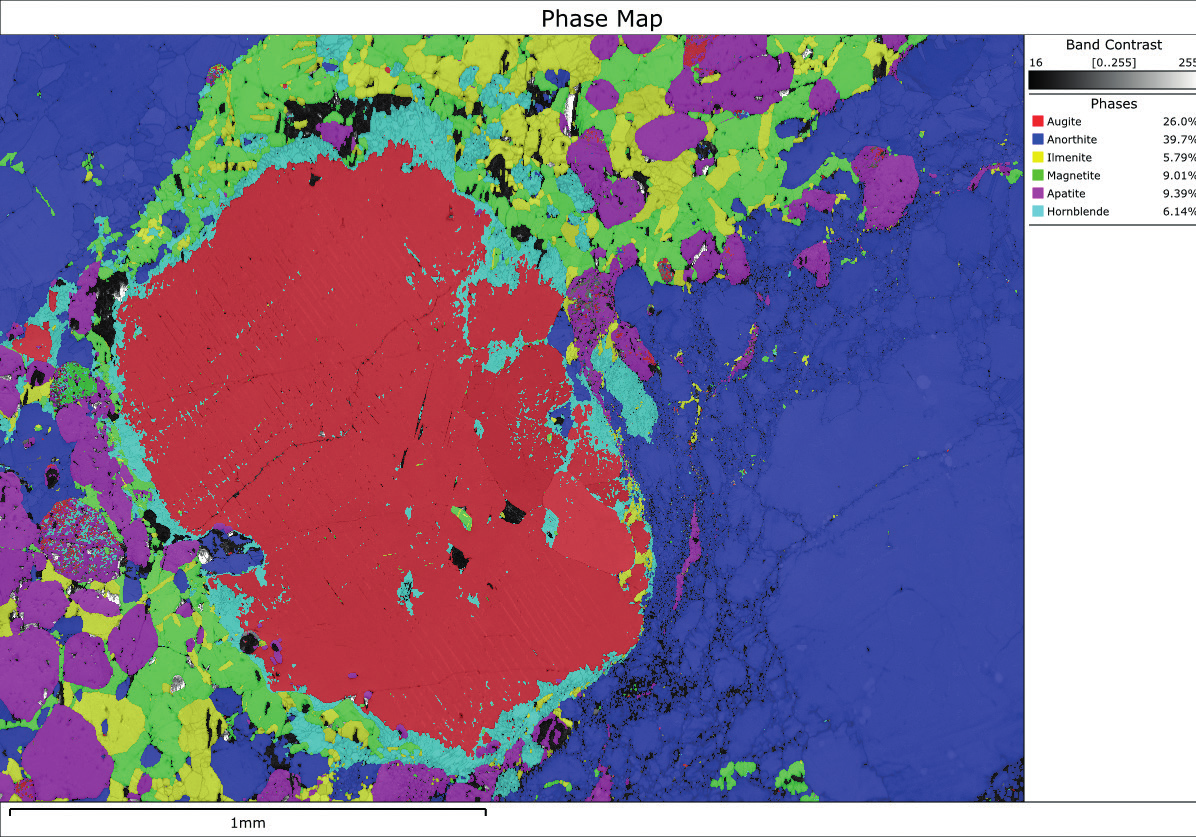
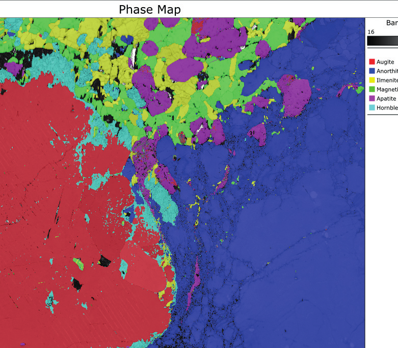
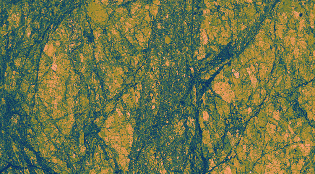
The conventional EBSD analysis resulted in relatively good quality data, although in the finest grained areas of the pseudotachylite vein the indexing rate was low. Overall, 67.7% of points could be indexed using the Hough transform approach. Reprocessing using the Refinement and Repair sweeps in MapSweeper significantly increased this hit rate, up to 83%, enabling a more detailed examination of the vein grain structures and mineral assemblage, as shown in the EBSD phase map. In addition, the better angular precision following MapSweeper refinement is clearly visible in the kernel average misorientation (KAM) maps. This angular precision improvement has important consequences when interpreting deformation structures: in the large clinozoisite grain in this area, the measured weighted Burgers vector orientations from the conventional data suggests a preferred <010> Burgers vector. However, in the improved data following pattern matching, analysis of the same grain indicates a preferred <001> Burgers vector. This difference is due to the removal of orientation imprecisions by the pattern matching process, and their corresponding impact (in the form of systematic artefacts) on disorientation and Burgers vector information.
 The TKD analysis was particularly challenging, with highly deformed and sub-µm sized grains producing very poor quality diffraction patterns. Most could not be reliably indexed using Hough-based indexing. Only the garnet grains could be indexed using the conventional approach; however, after the Indexing sweep in MapSweeper, the full phase distribution and grain structure in this area could be resolved. The results confirm recent studies, showing that most of the pseudotachylite vein is actually comprised of crystalline grains, albeit with high dislocation densities and grain sizes that cannot be resolved using light microscopy. Further examination reveals significant distortion within grains, and a close relationship between the orientation of larger (> 1 µm) grains and surrounding nanoscale grains, as exemplified by the hornblende pole figure.
 Summary
The EBSD and TKD results presented here are from an exceptionally challenging type of geological sample – a pseudotachylite vein. Despite the presence of up to 12 separate mineral phases, as well as a very fine grain size and high defect densities, the EBSD and TKD results were significantly enhanced by the application of MapSweeper data processing. For the EBSD dataset, the use of the Refinement and Repair sweep improved the data quality, enabling a better analysis of the phase distribution and detailed examination of deformation mechanisms within individual grains. In the TKD data, conventional indexing was unable to provide any reliable data, whereas DTM indexing in MapSweeper not only resolved the phases effectively but revealed extensive crystallographic orientation variations on the nanometre scale. These results suggest that the pseudotachylite vein structure may not be caused by frictional heating but involves crystal-plastic processes and possibly a degree of mechanical amorphisation. This type of study can only be achieved with the performance and versatility of AZtecCrystal MapSweeper.
Application Note: Resolving Defects and True Orientations in CIGS-Type Solar Cells
Introduction
Copper Indium Gallium Selenide (CIGS) thin films have for many years attracted significant interest from solar cell manufacturers due to their high efficiency and low cost. In addition, unlike conventional crystalline silicon solar cells, CIGS has a high absorption coefficient allowing thin films to be deposited onto flexible substrates in very thin layers (e.g. 1–2 µm).
Research has shown that the microstructural characteristics of the CIGS layer have a significant influence on a film's optoelectronic properties, with dislocation structures and antiphase domains playing an important role. However, the structure of Cu(In,Ga)Se2 poses particular challenges for effective measurement using routine electron backscatter diffraction (EBSD). Cu(In,Ga)Se2 has a tetragonal crystal structure, but with a c:a ratio of ~2.01, meaning that the structure is only ~0.5% away from having cubic symmetry. Conventional EBSD cannot resolve such small differences in the EBSD pattern and therefore each single Cu(In,Ga)Se2 crystal orientation will result in multiple measured orientations, all related by 90° rotations. In addition, these indexing errors will limit the angular precision of the EBSD measurements, making it impossible to resolve the all-important dislocation structures and antiphase domain boundaries in Cu(In,Ga)Se2 thin films.
Sample and Experimental Details
A 2.2 µm thick Cu(In,Ga)Se2 thin film, deposited on a Zn-doped GaAs (100) substrate, was cross-sectioned and then prepared using broad ion beam polishing. EBSD analyses were performed using a field emission gun scanning electron microscope (FEG-SEM) equipped with a Symmetry S3 EBSD detector and operating with a 15 keV beam energy. EBSD patterns were collected at 15 patterns per second using Symmetry's "Speed 1" mode (622 x 512 pixel resolution) from a 6.5 x 4 µm area with a 50 nm measurement step size. The patterns were initially indexed using AZtec's Refined Accuracy mode and saved for subsequent reanalysis.
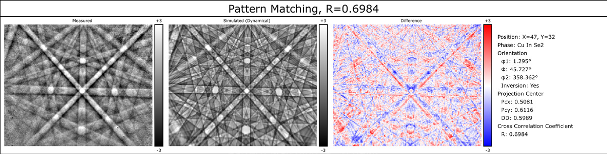
The data were reprocessed using AZtecCrystal MapSweeper: initial calibration refinement was performed on the cubic GaAs substrate and then the data were processed using MapSweeper's Refinement sweep, performed on 2x2 binned patterns and testing against all pseudosymmetrically-related orientations (90° rotation about both <100> and <010>) in order to resolve the true tetragonal symmetry. The final results were then saved and interrogated using AZtecCrystal.
 Results
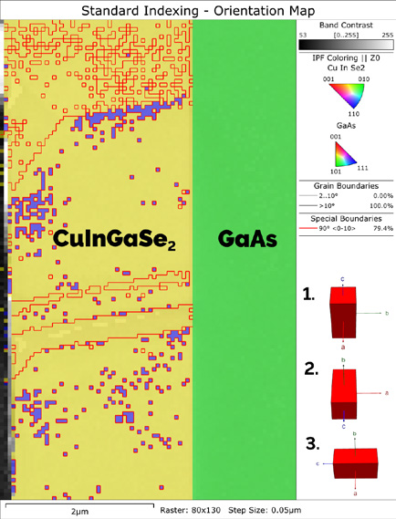
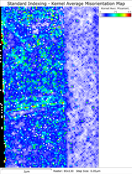
The original Hough-based indexing in AZtec could not reliably resolve the tetragonal structure of the Cu(In,Ga)Se2, resulting in a mix of 3 orientations in the CIGS layer as shown in the orientation map below. The lack of precision in this analysis is also clear in the Kernel Average Misorientation (KAM) map, highlighting local orientation changes of the crystal lattice (and therefore the presence of dislocation structures).
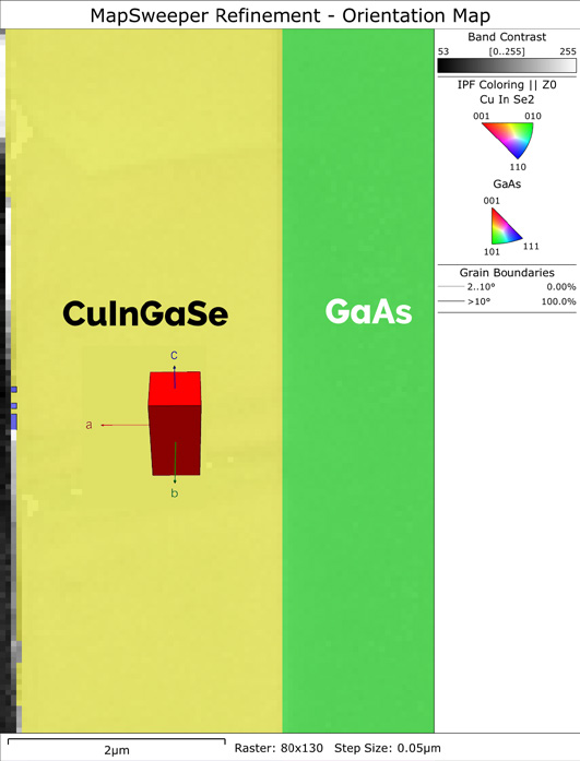
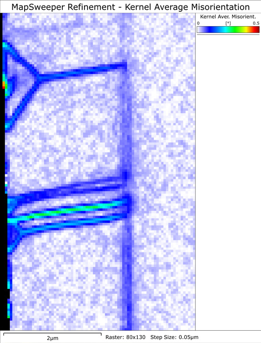
 Following the Refinement sweep in MapSweeper, the true tetragonal orientation of the CIGS layer has been resolved. X-ray diffraction analyses indicate that this orientation is linked to the Ga:In ratio (or the "GGI" value – Ga/(Ga+In)) in the thin film and so the improved measurements using MapSweeper enable this relationship to be tested. The significant improvement in angular precision is apparent in the KAM map; unlike in the conventional EBSD data, the MapSweeper refined data clearly show the presence of clear dislocation structures associated with antiphase domains.
 Summary
The refinement of EBSD data from a CIGS solar cell using AZtecCrystal MapSweeper has revealed the true tetragonal orientation of the crystal lattice and highlighted the presence of dislocation structures associated with antiphase domain boundaries. These were not visible following conventional EBSD analyses and demonstrate the power of hybrid pattern matching techniques within MapSweeper to reveal key microstructural features in such thin films, with corresponding implications for the optoelectronic performance of the material.